An optical link in four components
All four blocks come from the Abstract Components library: a CW Laser feeding a Mach‑Zehnder Modulator, a Photodiode at the output, and an electrical Source wired to the modulator's drive port. Optical connections are drawn in green, electrical ones in red.
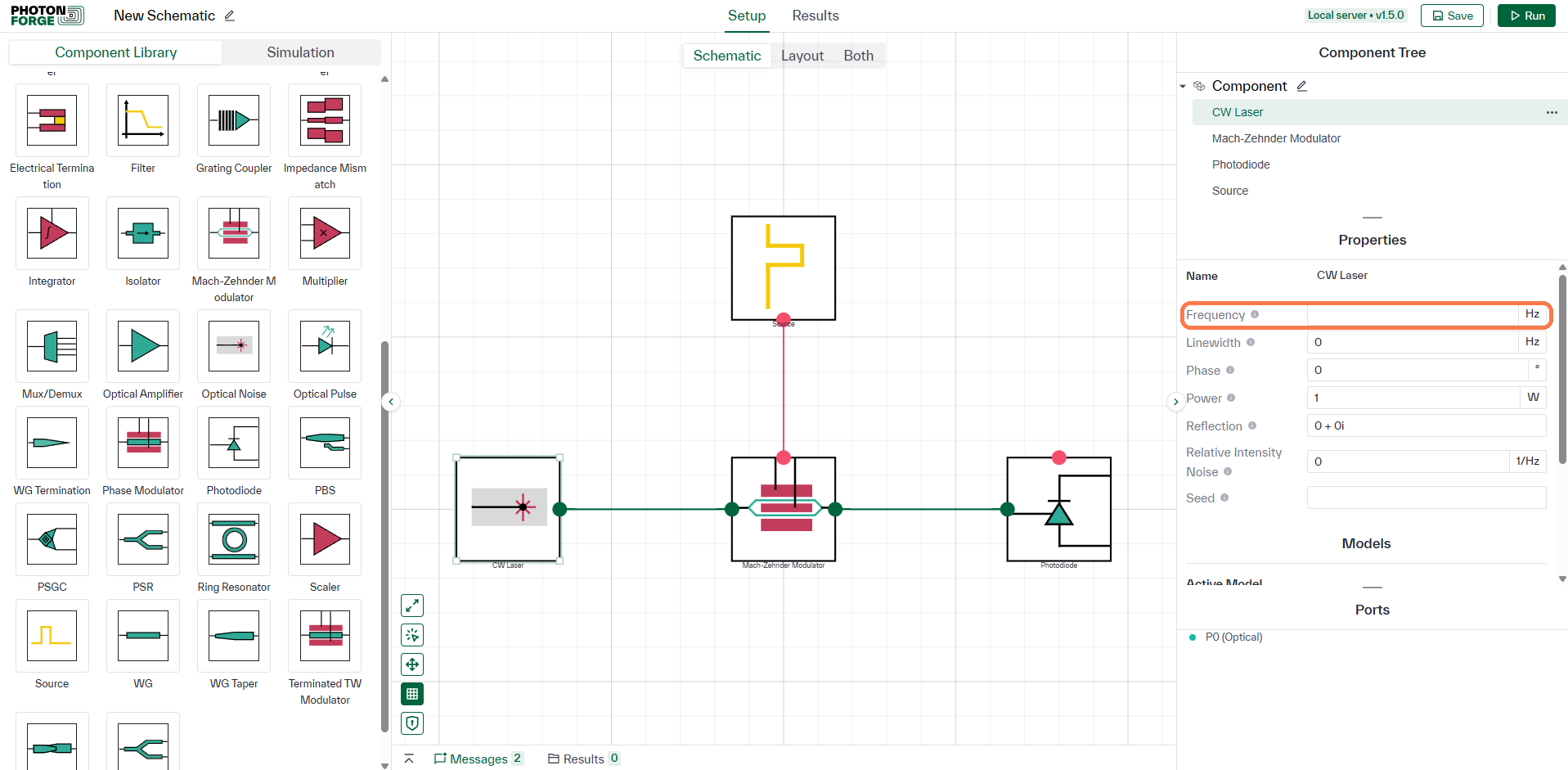
Tip: the laser's Frequency is left blank on purpose: it then defaults to the simulation's carrier frequency, which we will meet in the time-domain settings.
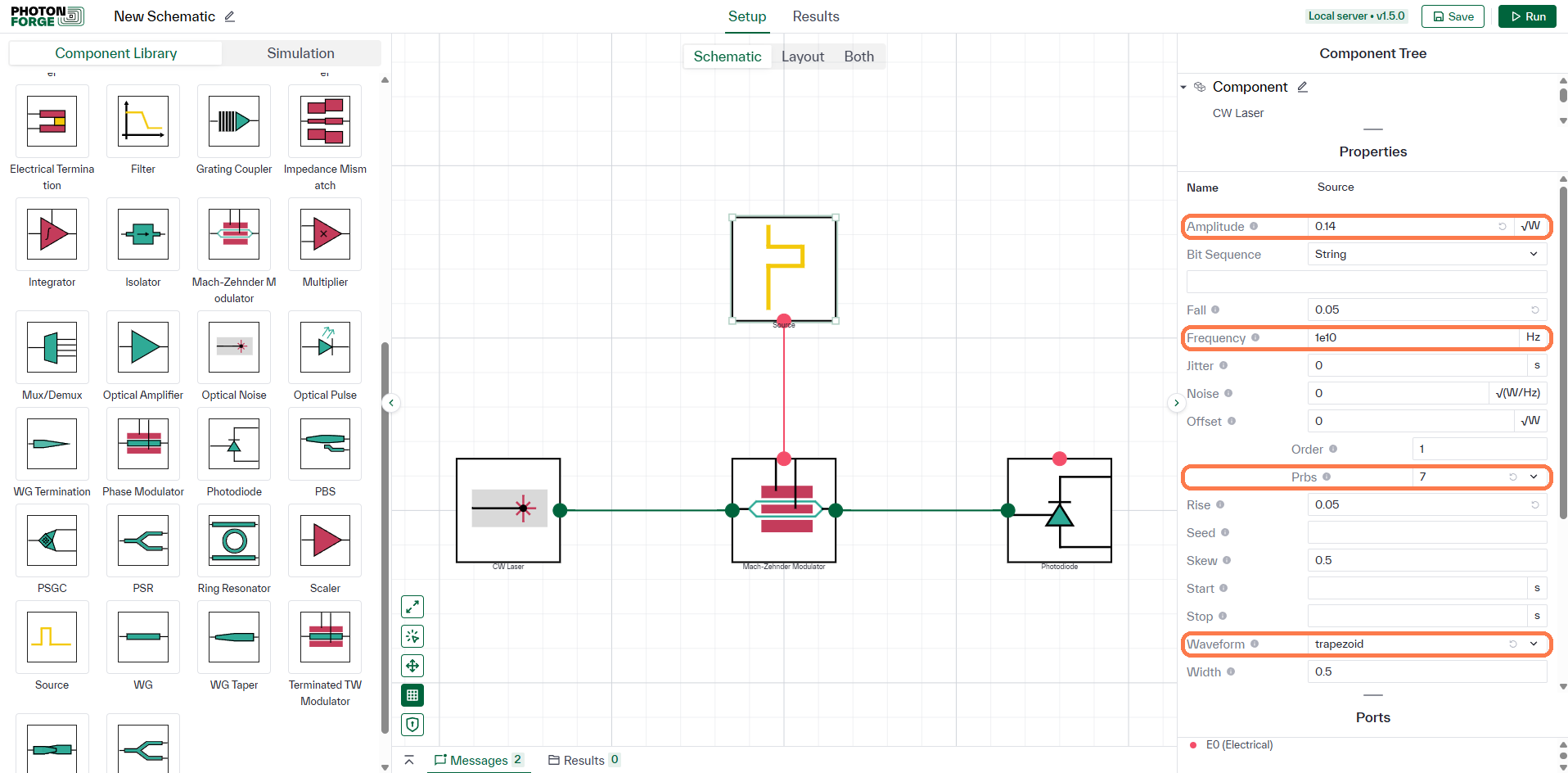
A 10 Gb/s pseudo-random bit source
Select the Source and set it up as an NRZ pattern generator: Frequency 1e10 (10 Gb/s), Prbs 7 (a 127‑bit pseudo‑random sequence), Waveform trapezoid with Rise and Fall of 0.05 bit periods, and Amplitude 0.14 ≈ 1/√50 √W: signals are expressed as power waves, so on the 50 Ω line this is exactly a 1 V drive.
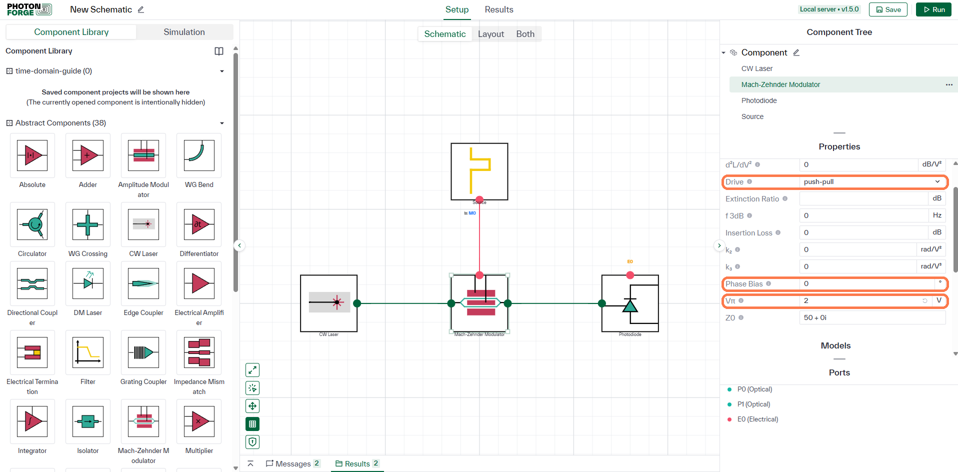
Push-pull drive against a 2 V Vπ
On the modulator, set Drive: push‑pull and Vπ = 2 V. In push‑pull operation the two arms are driven in opposite directions, so the 1 V source swing produces the full Vπ phase difference and takes the interferometer from maximum transmission all the way to extinction. Phase Bias stays at 0: the modulator transmits fully at zero drive, so a logical 1 switches the light off and the detected pattern will be the inverse of the bit stream.
Assign the circuit port at the photodiode
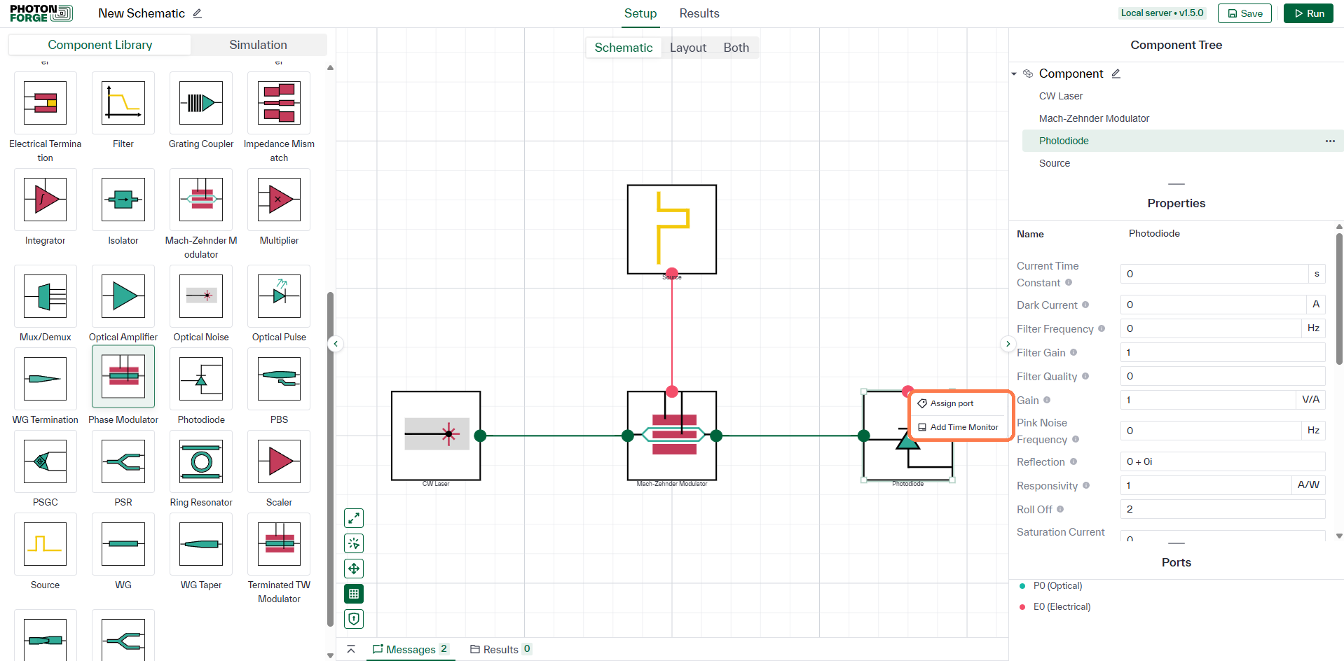
Right‑click the photodiode's electrical output and choose Assign port: the port becomes an external port of the circuit (labeled E0). Signals at assigned circuit ports are recorded automatically during a time‑domain run, so this one step already gives us the received waveform.
Add a Time Monitor on the drive
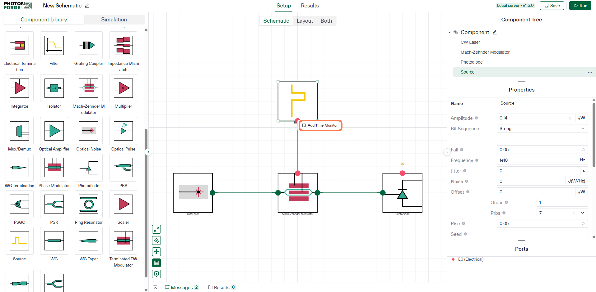
To compare the received data with what was sent, we also want the drive signal itself. Internal nodes are recorded with Time Monitors: right‑click the Source output and choose Add Time Monitor. A small M0 tag appears next to the port. You can monitor any optical or electrical connection this way.
Switch the mode to Time Domain
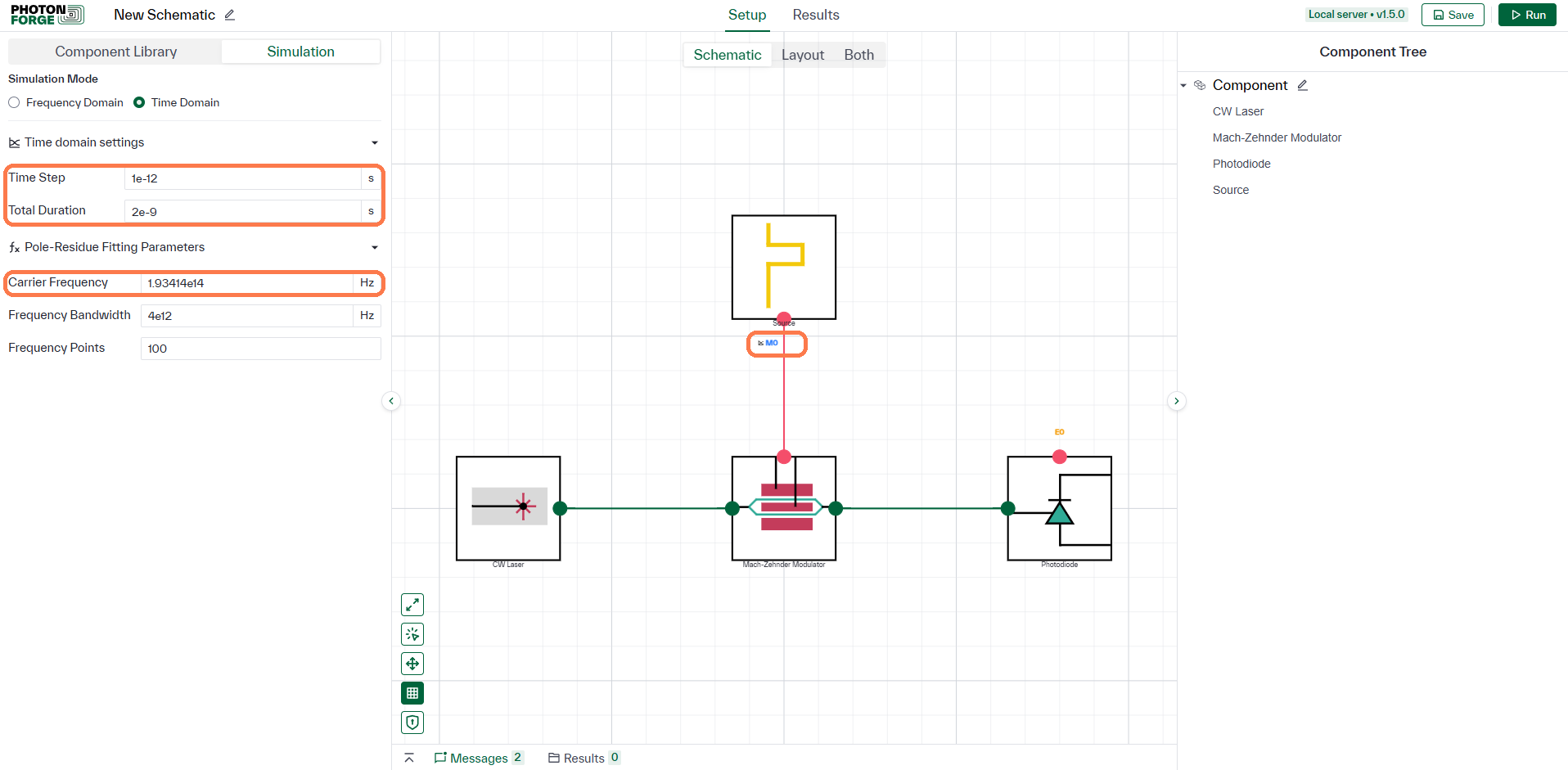
In the Simulation tab select Time Domain. Set Time Step 1e-12 (1 ps, giving 100 samples per bit) and Total Duration 2e-9 (2 ns, 20 bits). Under Pole‑Residue Fitting Parameters, the Carrier Frequency of 1.93414e14 Hz corresponds to 1550 nm: this is the optical carrier the blank laser frequency defaults to, and frequency‑defined models are fitted over the given bandwidth so they can be time‑stepped.
Run the time-domain simulation
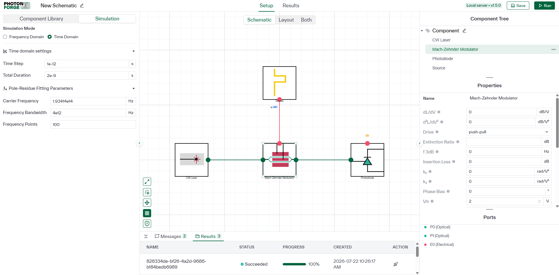
Click Run. The 2000‑step transient completes in seconds for this circuit of analytical models, and the job shows up as Succeeded in the Results panel.
Time Series join the data sets
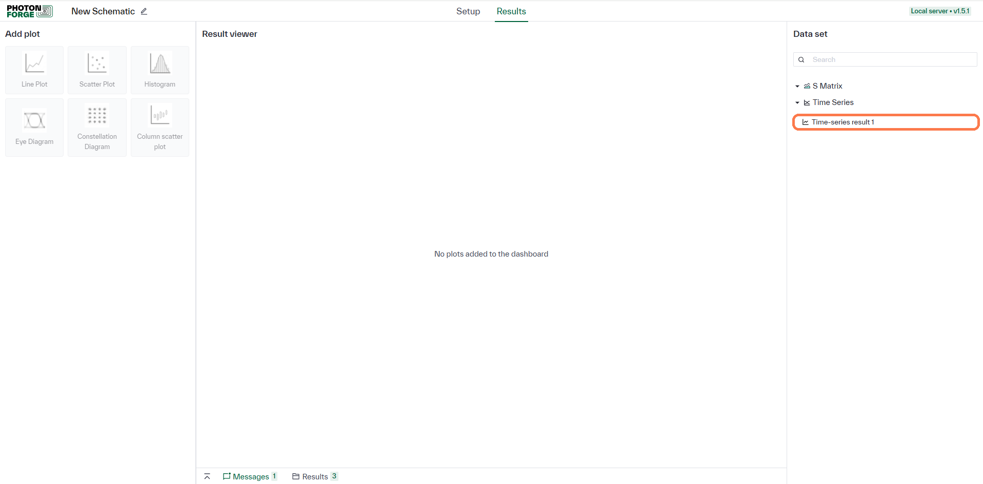
On the Results page the run appears under Data set → Time Series. Create a Line Plot from it: hover over the result, click the … button that appears and choose Create plot, or pick a plot type under Add plot and select the result from the dropdown.
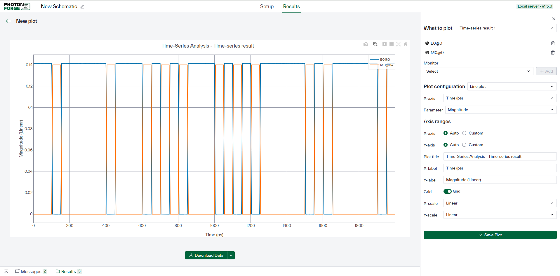
Sent bits, received bits
Add the two time series to the plot: E0@0, the received signal at the photodiode port, and M0@0+, the drive recorded by the monitor (the + denotes the outgoing signal). Both swing between 0 and 0.14 √W, that is 0 to 1 V on the 50 Ω line. The received trace is the logical inverse of the drive, exactly as predicted from the zero phase bias, with clean 100 ps bits and full extinction.