





from __future__ import annotations

import numpy as np
from matplotlib import pyplot as plt
from matplotlib.colors import LogNorm

import tidy3d as td
from tidy3d import web

td.config.logging.level = "ERROR"

# enable local subpixel averaging for accurate mode simulations (requires tidy3d[extras])
td.config.simulation.use_local_subpixel = True
TIDY3D
LEARNING CENTER
Example Library

GeSi electro-absorption modulator
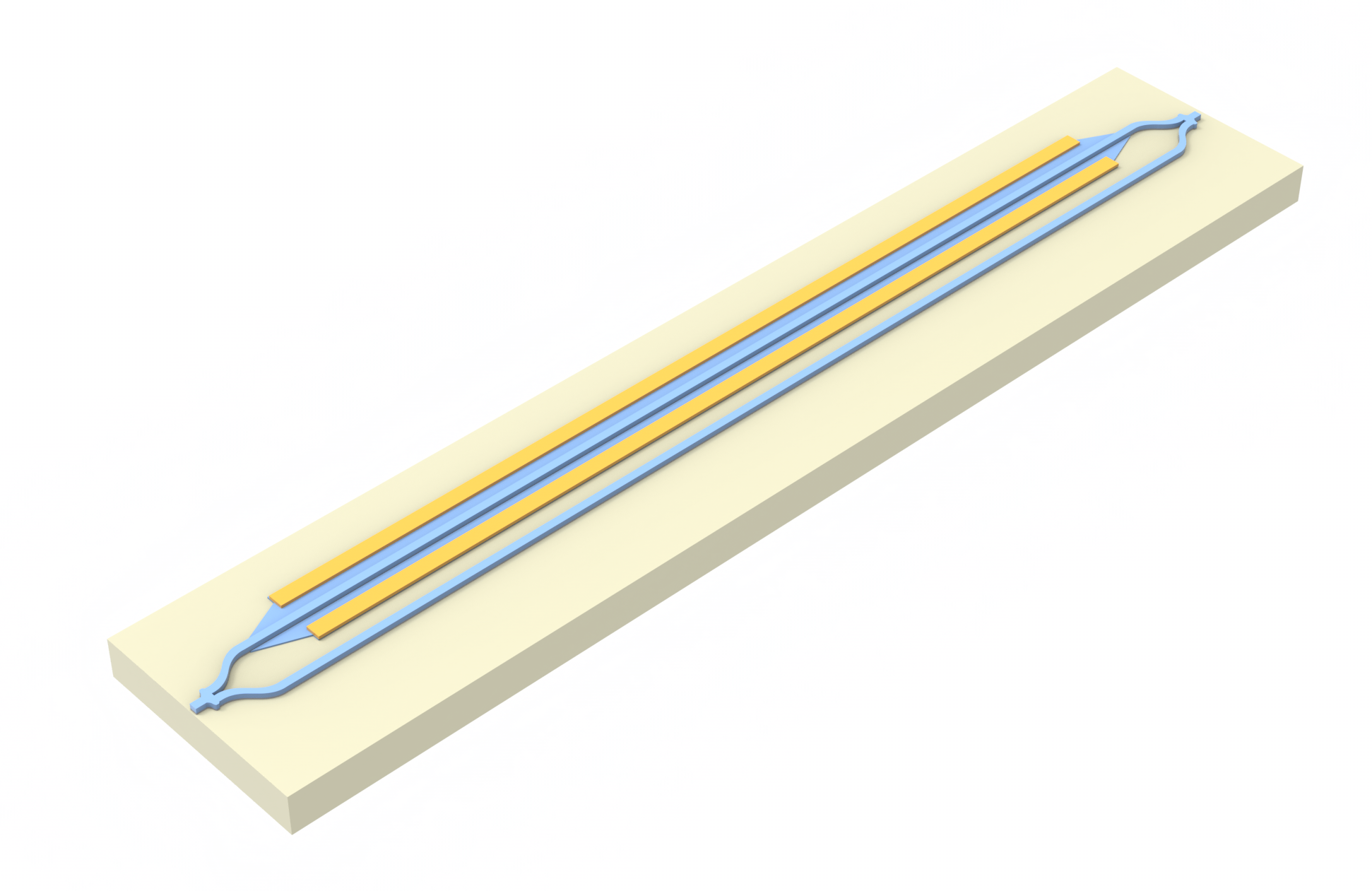
This notebook models the static electro-absorption performance of a GeSi electro-absorption modulator (EAM), following the device presented in Y. Liu, J. Sun, X. Li, S. Wang, W. Yue, Y. Cai, and M. Yu, “Thermally tunable GeSi electro-absorption modulator with a wide effective operating wavelength range,” Photonics Research 11(8), 1474 (2023). It is a horizontal PIN junction formed in a selectively grown \(\text{Ge}_{0.992}\text{Si}_{0.008}\) waveguide on a 220 nm silicon-on-insulator (SOI) platform.
The modulation mechanism is the Franz-Keldysh (FK) effect: an applied electric field tilts the semiconductor bands, which broadens the optical absorption edge and creates an absorption tail below the band gap. In an electro-absorption modulator, a reverse bias therefore raises the absorption at wavelengths just below the gap, switching the device between a low-loss (ON) and a high-loss (OFF) state.

The workflow couples a charge simulation to an optical mode solve:
- Solve the lateral PIN junction with the charge solver to obtain the electric field \(E(x, y)\) as a function of reverse bias.
- Apply the Franz-Keldysh model to convert \(E(x, y)\) into an absorption map \(\alpha(x, y)\) at each bias and wavelength.
- Build a spatially varying GeSi optical medium and solve the guided mode for every bias and wavelength.
- Extract the insertion loss (IL), extinction ratio (ER), and figure of merit (FOM = ER / IL).
Some geometric parameters and material properties are estimated based on typical values found in the literature. These are marked # estimated in the code.
Geometry Parameters
All dimensions are taken from the paper (Section 3 and Fig. 1a). Parameters marked with # estimated are not explicitly stated in the paper and follow a typical imec 220 nm SOI process.
# All dimensions in µm

# --- GeSi waveguide (from paper, Fig. 1a) ---
gesi_w = 0.60  # GeSi waveguide width (600 nm)
gesi_h = 0.35  # GeSi waveguide height (350 nm)
gesi_intrinsic_w = 0.45  # intrinsic region width (450 nm, Section 4)
device_length_um = 40.0  # device length along propagation (Section 4)

# --- Si rib waveguide (SOI, 220 nm platform) ---
si_rib_h = 0.22  # full Si rib height (220 nm)
si_rib_w = 0.80  # Si rib width (800 nm)
si_slab_h = 0.14  # Si slab height outside the rib (140 nm) # estimated
# GeSi is partially embedded in the rib; lateral contacts are in the 140 nm slab region
si_half_w = 2.5  # half-width of Si slab (estimated: ~5 µm total)  # estimated

# --- Doping concentrations ---
# GeSi doping (from paper, Section 4)
gesi_p_doping = 7e16  # acceptor concentration in GeSi p-side [cm^-3]
gesi_n_doping = 7e16  # donor concentration in GeSi n-side [cm^-3]
# Acceptors present in the as-grown GeSi without any intentional doping step.
# The paper does not report their concentration; this value is an assumption.
gesi_bg_doping = 1e16  # background acceptor concentration in the GeSi [cm^-3]

# Si slab doping (imec 220 nm SOI platform)
si_p_doping = 5e17  # Si p+ slab region [cm^-3]
si_pp_doping = 1e19  # Si p++ contact region [cm^-3]
si_n_doping = 5e17  # Si n+ slab region [cm^-3]
si_nn_doping = 1e19  # Si n++ contact region [cm^-3]
si_pp_width = 0.5  # p++ region width from left edge [µm]
si_nn_width = 0.5  # n++ region width from right edge [µm]
si_junction_x = 0.0  # x where the Si p implant meets the Si n implant [µm]

# --- Defective layer at the GeSi/Si growth interface ---
# The paper reports pre-existing defects at the Ge/Si and Ge/Ox interfaces but
# gives no thickness or density, so both values below are assumptions. Only the
# bottom (growth) Ge/Si interface is modeled here, not the GeSi sidewalls.
damaged_h = 0.02  # assumed thickness of the defective layer [µm]
tau_damaged = 1e-11  # assumed SRH lifetime in that layer [s]

# --- BOX and cladding ---
box_h = 2.0  # SiO2 BOX thickness (typical 220 nm SOI)  # estimated
clad_h = 0.92  # SiO2 cladding above GeSi

# --- Metal contacts ---
contact_w = 0.3  # metal contact width  # estimated

# --- Bias voltages to simulate ---
# the biases of the measured trace of Fig. 8(a), plus 0 V for the unbiased state
voltages = np.arange(-3.0, 1.0, 0.25)

# --- Derived quantities ---
sim_half_w = si_half_w + contact_w  # simulation half-width
z_size = 0.5  # structure z-extent for 2D simulation

# y-coordinates of key interfaces
y_bot = 0.0  # BOX / Si interface (bottom of Si)
y_slab_top = si_slab_h  # top of Si slab (= 0.14 µm)
y_rib_top = si_rib_h  # top of Si rib (= 0.22 µm)
y_gesi_top = si_rib_h / 2 + gesi_h  # top of GeSi (= 0.46 µm)
Material Definitions
GeSi Semiconductor Medium
The GeSi core is described by a SemiconductorMedium with Ge parameters (composition \(\text{Ge}_{0.992}\text{Si}_{0.008}\), 0.8% Si). The bandgap uses a VarshniEnergyBandGap and the mobilities use the CaugheyThomasMobility model.
The 0 K bandgap is linearly interpolated for 0.8% Si: \(E_{g0}(\mathrm{GeSi}) = (1-x)\,E_{g0}(\mathrm{Ge}) + x\,E_{g0}(\mathrm{Si})\) with \(x = 0.008\). Since \(x\) is very small, the Ge mobility and recombination parameters are used as-is.
The measured reverse current of this device rises by more than an order of magnitude between \(-1\) V and \(-3\) V, whereas a diffusion current saturates in reverse. At sufficiently large reverse voltages, field effects become dominant and have to be included, so the recombination list adds field-driven models to plain Shockley-Read-Hall:
-
HurkxTrapAssistedTunneling, passed as the
field_enhancementof the SRH model, shortens the SRH lifetimes where the field is high. Its inputs are the tunneling masses of the Ge L-valley electron and of the light hole. - HurkxDirectBandToBandTunneling, with Kane parameters for the 0.80 eV direct gap.
-
SelberherrImpactIonization, with Chynoweth coefficients for Ge. Use its
GradQuasiFermiform at a heterojunction: the driving force is then evaluated within a single material, so the band offset at the Ge/Si interface is not read as an accelerating field. - CanaliFieldDependence on both mobilities, for velocity saturation.
The electron affinities set the band offsets at the Ge/Si heterointerface (\(\Delta E_c \approx 0.05\) eV, \(\Delta E_v \approx 0.39\) eV). Thermionic emission across it uses the Richardson constant of each material, which the solver derives from its density of states.
x_si = 0.008  # Si fraction in GeSi

# Varshni parameters for Ge (indirect bandgap, used for transport)
eg0_ge = 0.7437  # eV
eg0_si = 1.16  # eV
# Linear interpolation for GeSi (for transport/carrier statistics)
eg0_gesi = (1 - x_si) * eg0_ge + x_si * eg0_si

# Electron affinities [eV]; the difference to Si sets the heterojunction band offsets
chi_si = 4.05
chi_gesi = (1 - x_si) * 4.00 + x_si * chi_si

# Ge density-of-states effective masses (m*/m0); not the tunneling masses used below
m_dos_n_gesi = 0.56  # conduction band
m_dos_p_gesi = 0.29  # valence band

# tunneling masses of the Ge L-valley electron and of the light hole
tat = td.HurkxTrapAssistedTunneling(m_t_n=0.12, m_t_p=0.043)

intrinsic_gesi = td.SemiconductorMedium(
    permittivity=16,  # Ge permittivity (x_si=0.008 → negligible change)
    N_c=td.IsotropicEffectiveDOS(m_eff=m_dos_n_gesi),
    N_v=td.IsotropicEffectiveDOS(m_eff=m_dos_p_gesi),
    E_g=td.VarshniEnergyBandGap(
        eg_0=eg0_gesi,  # bandgap at 0K, adjusted for 0.8% Si
        alpha=0.0004774,  # Varshni alpha for Ge [eV/K]
        beta=235,  # Varshni beta for Ge [K]
    ),
    electron_affinity=chi_gesi,
    mobility_n=td.CaugheyThomasMobility(
        mu_min=850,
        mu=3900,
        ref_N=2.6e17,
        exp_N=0.56,
        exp_1=0,
        exp_2=-1.66,
        exp_3=0,
        exp_4=0,
        field_dependence=td.CanaliFieldDependence(v_sat=6.0e6, beta=1.0),
    ),
    mobility_p=td.CaugheyThomasMobility(
        mu_min=300,
        mu=1800,
        ref_N=1e17,
        exp_N=1,
        exp_1=0,
        exp_2=-2.33,
        exp_3=0,
        exp_4=0,
        field_dependence=td.CanaliFieldDependence(v_sat=5.4e6, beta=1.0),
    ),
    R=[
        td.ShockleyReedHallRecombination(
            tau_n=td.FossumCarrierLifetime(
                tau_300=1e-9, alpha_T=0, A=1, B=0, C=0, N0=1e16, alpha=1
            ),
            tau_p=td.FossumCarrierLifetime(
                tau_300=1e-9, alpha_T=0, A=1, B=0, C=0, N0=1e16, alpha=1
            ),
            field_enhancement=tat,
        ),
        td.RadiativeRecombination(r_const=6.41e-14),
        td.AugerRecombination(c_n=1e-30, c_p=1e-30),
        # Kane parameters for the 0.80 eV direct gap
        td.HurkxDirectBandToBandTunneling(A=1e20, B=4.1e6, E_0=1, sigma=2),
        # Chynoweth coefficients for Ge
        td.SelberherrImpactIonization(
            alpha_n_inf=1.55e7,
            alpha_p_inf=1.0e7,
            E_n_crit=1.56e6,
            E_p_crit=1.28e6,
            beta_n=1.0,
            beta_p=1.0,
            formulation="GradQuasiFermi",
        ),
    ],
    delta_E_g=None,
)
Si Semiconductor Medium
The SOI slab lateral regions (p+/n+ implantation areas) use the built-in silicon charge model from the Tidy3D material library (cSi / Si_MultiPhysics), a SemiconductorMedium calibrated for silicon at 300 K. updated_copy adds the electron affinity the heterointerface needs and gives the silicon the same high-field models as the GeSi. Doping is applied the same way below.
# built-in silicon charge model from the Tidy3D material library
intrinsic_si = td.material_library["cSi"].variants["Si_MultiPhysics"].medium.charge
intrinsic_si = intrinsic_si.updated_copy(
    electron_affinity=chi_si,
    # velocity saturation in silicon
    mobility_n=intrinsic_si.mobility_n.updated_copy(
        field_dependence=td.CanaliFieldDependence(v_sat=1.07e7, beta=1.109)
    ),
    mobility_p=intrinsic_si.mobility_p.updated_copy(
        field_dependence=td.CanaliFieldDependence(v_sat=8.37e6, beta=1.213)
    ),
    # the same ionization model as the GeSi, with the silicon coefficients
    R=list(intrinsic_si.R)
    + [
        td.SelberherrImpactIonization(
            alpha_n_inf=7.03e5,
            alpha_p_inf=1.582e6,
            E_n_crit=1.23e6,
            E_p_crit=2.03e6,
            beta_n=1.0,
            beta_p=1.0,
            formulation="GradQuasiFermi",
        )
    ],
)
Doping Regions
The GeSi doping is stated in the paper (Section 4); the Si slab doping follows a typical imec 220 nm SOI process. Doping regions are defined with ConstantDoping boxes.
GeSi doping (from paper): - Whole film: 1×10¹⁶ cm⁻³ unintentional acceptor background, typical of epitaxial Ge - P-side: left 75 nm, 7×10¹⁶ cm⁻³ acceptors on top of the background - N-side: right 75 nm, 7×10¹⁶ cm⁻³ donors
Si slab doping (typical imec 220 nm SOI process): - P+ lateral region (left half, up to x = 0): 5×10¹⁷ cm⁻³ acceptors - P++ ohmic contact zone (leftmost 0.5 µm): 1×10¹⁹ cm⁻³ acceptors - N+ lateral region (right half, from x = 0): 5×10¹⁷ cm⁻³ donors - N++ ohmic contact zone (rightmost 0.5 µm): 1×10¹⁹ cm⁻³ donors
The p and n Si implants meet at the waveguide center, reproducing the abrupt Si junction of the device.
Each Si doping box spans the full Si height and covers both the slab and the exposed rib sidewall between the rib edge and the GeSi edge. Tidy3D applies a doping box only where the silicon medium exists, so the \(\text{SiO}_2\) regions are unaffected.
# --- GeSi doping (from paper) ---
# The boxes span the full GeSi height, from the embedded bottom (y_rib_top / 2) to the
# top (y_gesi_top), so the lower GeSi section inside the Si rib is doped as well.
p_doping_gesi = td.ConstantDoping.from_bounds(
    concentration=gesi_p_doping,
    rmin=(-gesi_w / 2, y_rib_top / 2 - 1e-4, -z_size),
    rmax=(-gesi_intrinsic_w / 2, y_gesi_top + 1e-4, z_size),
)
n_doping_gesi = td.ConstantDoping.from_bounds(
    concentration=gesi_n_doping,
    rmin=(+gesi_intrinsic_w / 2, y_rib_top / 2 - 1e-4, -z_size),
    rmax=(+gesi_w / 2, y_gesi_top + 1e-4, z_size),
)
# unintentional acceptor background over the whole GeSi film; the wing implants add on top
bg_doping_gesi = td.ConstantDoping.from_bounds(
    concentration=gesi_bg_doping,
    rmin=(-gesi_w / 2 - 1e-4, y_rib_top / 2 - 1e-4, -z_size),
    rmax=(+gesi_w / 2 + 1e-4, y_gesi_top + 1e-4, z_size),
)

# --- Si doping ---

p_doping_si = td.ConstantDoping.from_bounds(
    concentration=si_p_doping,
    rmin=(-si_half_w, y_bot - 1e-4, -z_size),
    rmax=(si_junction_x, y_rib_top + 1e-4, z_size),
)
pp_doping_si = td.ConstantDoping.from_bounds(
    concentration=si_pp_doping,
    rmin=(-si_half_w, y_bot - 1e-4, -z_size),
    rmax=(-si_half_w + si_pp_width, y_rib_top + 1e-4, z_size),  # full Si height
)
n_doping_si = td.ConstantDoping.from_bounds(
    concentration=si_n_doping,
    rmin=(si_junction_x, y_bot - 1e-4, -z_size),
    rmax=(+si_half_w, y_rib_top + 1e-4, z_size),
)
nn_doping_si = td.ConstantDoping.from_bounds(
    concentration=si_nn_doping,
    rmin=(+si_half_w - si_nn_width, y_bot - 1e-4, -z_size),
    rmax=(+si_half_w, y_rib_top + 1e-4, z_size),  # full Si height
)
Multiphysics Mediums and Structures
The doped semiconductors, the \(\text{SiO}_2\) cladding, and the metal contacts are combined into MultiPhysicsMedium objects (charge and optical properties) and assigned to Structure objects. A second GeSi medium, identical except for the shortened SRH lifetime, covers the first 20 nm above the growth interface. It stands for the interface defects reported in the paper; its thickness and lifetime are assumptions rather than measured values, and they set the magnitude of the reverse current, so they are the first thing to vary when comparing against a measurement.
# --- Build doped semiconductor mediums ---
doped_gesi = intrinsic_gesi.updated_copy(
    N_a=[p_doping_gesi, bg_doping_gesi],
    N_d=[n_doping_gesi],
)
doped_si = intrinsic_si.updated_copy(
    N_a=[p_doping_si, pp_doping_si],
    N_d=[n_doping_si, nn_doping_si],
)

# --- MultiPhysicsMedium ---
GeSi = td.MultiPhysicsMedium(
    charge=doped_gesi, optical=td.material_library["Ge"]["Nunley"], name="GeSi"
)
# same medium with only the SRH lifetimes shortened
tau_dam = td.FossumCarrierLifetime(
    tau_300=tau_damaged, alpha_T=0, A=1, B=0, C=0, N0=1e16, alpha=1
)
GeSiDamaged = td.MultiPhysicsMedium(
    charge=doped_gesi.updated_copy(
        R=[
            r.updated_copy(tau_n=tau_dam, tau_p=tau_dam)
            if isinstance(r, td.ShockleyReedHallRecombination)
            else r
            for r in doped_gesi.R
        ]
    ),
    optical=td.material_library["Ge"]["Nunley"],
    name="GeSi_damaged",
)
Si = td.MultiPhysicsMedium(
    charge=doped_si, optical=td.material_library["cSi"]["Palik_Lossless"], name="Si"
)
SiO2 = td.MultiPhysicsMedium(
    charge=td.ChargeInsulatorMedium(permittivity=3.9),
    optical=td.material_library["SiO2"]["Horiba"],
    name="SiO2",
)
Metal = td.MultiPhysicsMedium(
    charge=td.ChargeConductorMedium(conductivity=1),
    optical=td.Medium(permittivity=1),
    name="Metal",
)

# --- Structure objects ---
# SiO2 background (BOX + cladding)
sio2_struct = td.Structure(
    geometry=td.Box.from_bounds(
        rmin=(-sim_half_w, -box_h, -z_size),
        rmax=(+sim_half_w, y_gesi_top + clad_h, z_size),
    ),
    medium=SiO2,
    name="sio2_struct",
)
# Si SLAB: thin (140 nm), full lateral width — carries P/N doping on sides
si_slab = td.Structure(
    geometry=td.Box.from_bounds(
        rmin=(-si_half_w, y_bot, -z_size), rmax=(+si_half_w, y_slab_top, z_size)
    ),
    medium=Si,
    name="si_slab",
)
# Si RIB: full 220 nm, 800 nm wide — overlaps slab in the center, intrinsic (no doping boxes here)
si_rib = td.Structure(
    geometry=td.Box.from_bounds(
        rmin=(-si_rib_w / 2, y_bot, -z_size), rmax=(+si_rib_w / 2, y_rib_top, z_size)
    ),
    medium=Si,
    name="si_rib",
)
# GeSi waveguide: 600 nm wide, 350 nm tall, partially embedded in the Si rib
gesi_struct = td.Structure(
    geometry=td.Box.from_bounds(
        rmin=(-gesi_w / 2, y_rib_top / 2, -z_size),
        rmax=(+gesi_w / 2, y_gesi_top, z_size),
    ),
    medium=GeSi,
    name="gesi_struct",
)
# damaged GeSi layer over the first 20 nm above the growth interface
gesi_damaged_struct = td.Structure(
    geometry=td.Box.from_bounds(
        rmin=(-gesi_w / 2, y_rib_top / 2, -z_size),
        rmax=(+gesi_w / 2, y_rib_top / 2 + damaged_h, z_size),
    ),
    medium=GeSiDamaged,
    name="gesi_damaged",
)
# Metal contacts ON TOP of p++/n++ Si slab regions (above y = y_slab_top)
contact_p = td.Structure(
    geometry=td.Box.from_bounds(
        rmin=(-si_half_w, y_slab_top, -z_size),
        rmax=(-si_half_w + si_pp_width, y_slab_top + contact_w, z_size),
    ),
    medium=Metal,
    name="contact_p",
)
contact_n = td.Structure(
    geometry=td.Box.from_bounds(
        rmin=(+si_half_w - si_nn_width, y_slab_top, -z_size),
        rmax=(+si_half_w, y_slab_top + contact_w, z_size),
    ),
    medium=Metal,
    name="contact_n",
)

# Order matters: later structures override earlier ones in overlapping regions
structures = [
    sio2_struct,
    si_slab,
    si_rib,
    gesi_struct,
    gesi_damaged_struct,
    contact_p,
    contact_n,
]
# Build Scene and visualize doping + structure layout
scene = td.Scene(
structures=structures,
)
fig, axes = plt.subplots(1, 2, figsize=(14, 4))
scene.plot(z=0, ax=axes[0])
axes[0].set_title("Structure cross-section")
scene.plot_structures_property(z=0, property="doping", ax=axes[1], scale="symlog")
axes[1].set_title("Doping map")
plt.tight_layout()
plt.show()
Boundary Conditions
The p-contact (left metal) is swept from \(-3\) V to \(+0.75\) V (negative = reverse bias, \(V_p < V_n\)); the n-contact (right metal) is held at 0 V. The voltage boundary condition is placed at the interface between the metal contact and the Si slab, using VoltageBC with a DCVoltageSource.
bc_p = td.HeatChargeBoundarySpec(
    placement=td.StructureStructureInterface(structures=[contact_p.name, si_slab.name]),
    condition=td.VoltageBC(source=td.DCVoltageSource(voltage=voltages)),
)
bc_n = td.HeatChargeBoundarySpec(
    placement=td.StructureStructureInterface(structures=[contact_n.name, si_slab.name]),
    condition=td.VoltageBC(source=td.DCVoltageSource(voltage=0.0)),
)
bcs = [bc_p, bc_n]
Monitors
We record the junction capacitance (SteadyCapacitanceMonitor) and the electric field (SteadyElectricFieldMonitor).
capacitance_mnt = td.SteadyCapacitanceMonitor(
    center=(0, 0, 0),
    size=(td.inf, td.inf, 0),
    name="capacitance_mnt",
)
# Electric field monitor over the GeSi region — directly provides E = -grad(phi) [V/µm]
efield_mnt = td.SteadyElectricFieldMonitor(
    center=(0, (y_rib_top / 2 + y_gesi_top) / 2, 0),
    size=(gesi_w + 0.2, gesi_h + 0.1, 0),
    name="efield_mnt",
)
monitors = [capacitance_mnt, efield_mnt]
Mesh, Convergence, and Simulation
The mesh uses an AutoUnstructuredGrid: the reference resolution sets the interface spacing, while a uniform grid in each semiconductor medium resolves the PIN junction. The bulk mesh uses the default four-times-coarser spacing. The ChargeToleranceSpec is tightened to resolve the small reverse-bias currents. The DC bias sweep is defined by an IsothermalSteadyChargeDCAnalysis, and everything is assembled into a HeatChargeSimulation.
# Mesh: uniform grid inside the semiconductors, refined near material interfaces.
mesh_resolution = 0.01
mesh_spec = td.AutoUnstructuredGrid(
    dl_reference=mesh_resolution,
    uniform_grid_mediums=[GeSi.name, GeSiDamaged.name, Si.name],
)

# the small reverse-bias currents need a tight rel_tol, and at this tolerance the
# linear solver needs more preconditioner_iterations than the default
convergence_settings = td.ChargeToleranceSpec(rel_tol=1e-13, preconditioner_iterations=100)

analysis_type = td.IsothermalSteadyChargeDCAnalysis(
    temperature=300.0,
    convergence_dv=0.5,
    tolerance_settings=convergence_settings,
    fermi_dirac=True,
)

sim = td.HeatChargeSimulation.from_scene(
    scene=scene,
    size=(2 * sim_half_w, box_h + y_gesi_top + clad_h, 0),
    center=(0, (y_gesi_top + clad_h - box_h) / 2, 0),
    monitors=monitors,
    grid_spec=mesh_spec,
    boundary_spec=bcs,
    analysis_spec=analysis_type,
)
# Visualize simulation cross-section (zoomed into the waveguide region)
fig, ax = plt.subplots(figsize=(8, 5))
sim.plot_property(z=0, property="electric_conductivity", ax=ax, monitor_alpha=0)
ax.set_ylim(-0.1, 0.8)
ax.set_title("Simulation cross-section (conductivity map)")
plt.show()
Run Simulation
The charge simulation is submitted to the cloud with web.run.
charge_data = web.run(
    sim,
    task_name="GeSiEAM_charge",
    path="gesi_eam_charge_data.hdf5",
)
08:33:34 UTC Created task 'GeSiEAM_charge_mesh' with resource_id
'vom-8abedcf2-6ba1-42a2-bb88-3d172bb108e6' and task_type
'VOLUME_MESH'.
Tidy3D's VolumeMesher solver is currently in the beta stage. Cost
of VolumeMesher simulations is subject to change in the future.
↑ simulation.hdf5.gz ━━━━━━━━━━━━━━━━━━━━━━━━━ 100.0% • 3.5/3.5 kB • ? • 0:00:00
08:33:36 UTC Estimated FlexCredit cost: 0.025. Use 'web.real_cost(task_id)' to
get the billed FlexCredit cost after a simulation run.
08:33:37 UTC status = queued
To cancel the simulation, use 'web.abort(task_id)' or
'web.delete(task_id)' or abort/delete the task in the web UI.
Terminating the Python script will not stop the job running on the
cloud.
08:33:42 UTC starting up solver
running solver
08:33:49 UTC status = success
Created task 'GeSiEAM_charge_solve' with resource_id
'hec-9ee403f7-d6a1-418f-90e0-16fd471673d9' and task_type
'HEAT_CHARGE'.
Tidy3D's HeatCharge solver is currently in the beta stage. Cost of
HeatCharge simulations is subject to change in the future.
↑ simulation.hdf5.gz ━━━━━━━━━━━━━━━━━━━━━━━━━ 100.0% • 3.5/3.5 kB • ? • 0:00:00
08:33:50 UTC Estimated typical FlexCredit cost: 0.056. For charge simulations,
the billed cost depends on the number of solver iterations required
for convergence.
Maximum FlexCredit cost: 16.658. This assumes the charge solver
reaches its configured iteration limits for all applied biases. Use
'web.real_cost(task_id)' to get the billed FlexCredit cost after a
simulation run.
08:33:52 UTC status = queued
To cancel the simulation, use 'web.abort(task_id)' or
'web.delete(task_id)' or abort/delete the task in the web UI.
Terminating the Python script will not stop the job running on the
cloud.
08:33:57 UTC status = preprocess
08:34:17 UTC starting up solver
08:34:18 UTC running solver
08:35:52 UTC status = queued
08:37:38 UTC status = preprocess
08:37:51 UTC status = running
08:40:09 UTC status = queued
08:42:11 UTC status = preprocess
08:42:30 UTC status = running
08:43:02 UTC status = queued
08:43:07 UTC status = preprocess
08:43:23 UTC status = running
08:56:20 UTC status = queued
08:57:43 UTC status = preprocess
08:57:59 UTC status = running
09:14:22 UTC status = success
↓ simulation_data.hdf5.gz ━━━━━━━━━━━━ 100.0% • 637.3/637.3 • 2.6 MB/s • 0:00:00
kB
09:14:25 UTC Loading results from gesi_eam_charge_data.hdf5 Post-Processing: Electric Field
Extract the electric field magnitude in the GeSi intrinsic region as a function of reverse bias. The field is read from the SteadyElectricFieldMonitor, interpolated onto a regular grid over the full height of the intrinsic GeSi, the region the Franz-Keldysh model uses below, and averaged. The paper estimates about 12 kV/cm built-in and about 74 kV/cm at \(-3\) V for a uniform field across the 450 nm intrinsic region. The two-dimensional solution is lower and non-uniform, with only part of the applied bias dropping across the intrinsic GeSi.
E_data = charge_data[efield_mnt.name].E  # unstructured; components along 'axis'

# |E| maps on a regular grid over the GeSi cross-section, for a subset of biases
x_map = np.linspace(-0.4, 0.4, 161)
y_map = np.linspace(y_rib_top / 2 - 0.05, y_gesi_top + 0.05, 101)
E_map = E_data.interp(x=x_map, y=y_map, z=0.0)
E_map_mag = np.sqrt(E_map.sel(axis=0) ** 2 + E_map.sel(axis=1) ** 2).squeeze("z") * 10  # kV/cm

# log color scale: the field spans two decades between the intrinsic region and
# the Ge/Si interface
plot_voltages = [-3.0, -1.0, 0.0, 0.75]
fig, axes = plt.subplots(2, 2, figsize=(9, 7))
for ax, v in zip(axes.ravel(), plot_voltages):
    E_map_mag.sel(voltage=v, method="nearest").plot(
        x="x",
        y="y",
        ax=ax,
        cmap="viridis",
        norm=LogNorm(vmin=1, vmax=1e3),
        cbar_kwargs={"label": "|E| [kV/cm]"},
    )
    ax.set_aspect("equal")
    ax.set_title(f"V = {v} V")
plt.suptitle("Electric field in the GeSi region", y=1.02)
plt.tight_layout()
plt.show()
# regular grid over the intrinsic GeSi, full height from the embedded bottom to the top
x_int = np.linspace(-gesi_intrinsic_w / 2, gesi_intrinsic_w / 2, 60)
y_int = np.linspace(y_rib_top / 2, y_gesi_top, 60)

# Tidy3D native interpolation of the unstructured field onto the grid
Eg = E_data.interp(x=x_int, y=y_int, z=0.0)
E_mag = np.sqrt(Eg.sel(axis=0) ** 2 + Eg.sel(axis=1) ** 2).squeeze("z")  # |E|(x,y,voltage)

print(f"{'V_bias (V)':>12} | {'E_avg (kV/cm)':>16}")
print("-" * 32)
for v in voltages:
    e_avg_kv_cm = float(E_mag.sel(voltage=v, method="nearest").mean()) * 1e6 / 1e5  # V/µm -> kV/cm
    print(f"{v:>12.2f} | {e_avg_kv_cm:>16.1f}")
V_bias (V) | E_avg (kV/cm)
--------------------------------
-3.00 | 26.6
-2.75 | 26.5
-2.50 | 25.9
-2.25 | 25.7
-2.00 | 25.1
-1.75 | 23.7
-1.50 | 21.5
-1.25 | 19.3
-1.00 | 17.4
-0.75 | 15.7
-0.50 | 14.2
-0.25 | 13.0
0.00 | 11.0
0.25 | 7.6
0.50 | 4.3
0.75 | 2.0Dark Current
The terminal (dark) current from the DC analysis is compared with the measurement of Fig. 8(a), digitized from the published figure. For a 2D (z = 0) simulation, the current is reported per unit length, so it is scaled by the 40 µm device length. The printed values compare the current at \(-3\) V and the \(I(-3)/I(-1)\) ratio with the measurement.
# dark current digitized from Fig. 8(a) of the paper
V_meas = np.array(
    [-3.0, -2.75, -2.5, -2.25, -2.0, -1.75, -1.5, -1.25, -1.0, -0.75, -0.5, -0.25, 0.25, 0.5, 0.75]
)
I_meas_A = np.array(
    [2.23e-7, 1.90e-7, 1.57e-7, 1.22e-7, 9.06e-8, 6.55e-8, 4.46e-8, 2.89e-8,
     1.79e-8, 9.90e-9, 6.14e-9, 4.16e-9, 1.43e-6, 1.01e-4, 7.39e-4]
)

I_per_um = np.abs(charge_data.device_characteristics.steady_dc_current_voltage)  # [A/µm]
V_all = I_per_um.coords["v"].values
I_all_A = I_per_um.values * device_length_um  # [A]
# 0 V is excluded: the net terminal current vanishes at equilibrium
nonzero = V_all != 0.0
V_sim, I_sim_A = V_all[nonzero], I_all_A[nonzero]

fig, ax = plt.subplots(figsize=(6.5, 4.5))
ax.semilogy(V_meas, I_meas_A, "ro", ms=5, mfc="none", label="measured (Fig. 8a)")
ax.semilogy(V_sim, I_sim_A, "ks-", ms=5, label="simulated")
ax.set_xlabel("Applied bias (V)")
ax.set_ylabel("Dark current (A)")
ax.set_title("Dark current vs bias")
ax.set_ylim(1e-10, 1e-3)
ax.legend()
ax.grid(True, which="both", alpha=0.3)
plt.tight_layout()
plt.show()

i_sim_3 = float(I_sim_A[np.isclose(V_sim, -3.0)][0])
i_sim_1 = float(I_sim_A[np.isclose(V_sim, -1.0)][0])
i_meas_3, i_meas_1 = I_meas_A[0], I_meas_A[8]
print(f"I(-3 V): simulated {i_sim_3 * 1e9:.1f} nA, measured {i_meas_3 * 1e9:.1f} nA")
print(f"I(-3)/I(-1): simulated {i_sim_3 / i_sim_1:.2f}, measured {i_meas_3 / i_meas_1:.2f}")
I(-3 V): simulated 539.4 nA, measured 223.0 nA
I(-3)/I(-1): simulated 25.56, measured 12.46
The model reaches the measured order of magnitude at \(-3\) V and under-predicts how steeply the current rises with reverse bias. Both depend on inputs the paper does not give, above all the thickness and lifetime of the defective layer, the acceptor background of the GeSi, and the resolution of the interface mesh, with the low-bias current the more sensitive of the two.
Franz-Keldysh Optical Modulation
With the electric field known, the Franz-Keldysh absorption map \(\alpha(x, y)\) is computed at each bias and wavelength, converted to an imaginary index \(k(x, y)\), and used to build a spatially varying GeSi CustomMedium. The guided mode is then solved for every bias and wavelength with a ModeSimulation to obtain IL, ER, and FOM.
The absorption coefficient follows the Franz-Keldysh model of the paper (light- and heavy-hole contributions):
\[\alpha(\omega, T) = \frac{e^2 E_p(T)}{12 n_r c \varepsilon_0 m_0 \omega} \left\{ \frac{(2 m_{r,lh})^{3/2}}{\hbar^2} \sqrt{\hbar\theta_{F,lh}} \left[ -\eta_{lh}(T) \mathrm{Ai}^2(\eta_{lh}(T)) + \mathrm{Ai}'^{2}(\eta_{lh}(T)) \right] + \frac{(2 m_{r,hh})^{3/2}}{\hbar^2} \sqrt{\hbar\theta_{F,hh}}\left[ -\eta_{hh}(T) \mathrm{Ai}^2(\eta_{hh}(T)) + \mathrm{Ai}'^{2}(\eta_{hh}(T)) \right] \right\}\]
def FranzKeldysh(omega, E_field, n_r, E_p, m_e_Gamma, m_lh, m_hh, E_gd, DeltaE_g_lh, DeltaE_g_hh):
    # E_field     : applied electric field                     [V/µm]

    # Material parameters
    # omega       : optical angular frequency                  [rad/s]
    # n_r         : refractive index                           [dimensionless]
    # E_p         : Kane energy (matrix constant)              [eV]
    # m_e_Gamma   : electron effective mass at the Γ valley    [eV·s²/µm²]  (= (m*/m0)·M_E_EV)
    # m_lh        : light-hole effective mass                  [eV·s²/µm²]
    # m_hh        : heavy-hole effective mass                  [eV·s²/µm²]
    # E_gd        : direct bandgap                            [eV]
    # DeltaE_g_lh : strain-induced gap shift (light hole)      [eV]
    # DeltaE_g_hh : strain-induced gap shift (heavy hole)      [eV]

    # constants
    e = 1  # elementary charge = 1 (eV unit system)
    c = td.C_0  # speed of light [µm/s]
    m_0 = td.constants.M_E_EV  # free-electron mass [eV·s²/µm²]  (= M_E_C_SQUARE / C_0²)
    hbar = td.HBAR  # reduced Planck constant [eV·s]
    eps0 = td.EPSILON_0 / td.Q_e  # F/µm (Coulomb) -> elementary-charge unit (factor 1/e)

    # Airy functions
    from scipy.special import airy

    def Airy(x):
        return airy(x)[0]  # Ai(x)

    def Airy2(x):
        return airy(x)[1]  # Ai'(x)

    # effective mass
    m_r_lh = m_e_Gamma * m_lh / (m_e_Gamma + m_lh)  # reduced e-h mass, light  [eV·s²/µm²]
    m_r_hh = m_e_Gamma * m_hh / (m_e_Gamma + m_hh)  # reduced e-h mass, heavy  [eV·s²/µm²]

    # hbarTheta
    hbarTheta_cte = (hbar**2) * (e**2) * (E_field**2)
    hbarTheta_lh = ((hbarTheta_cte) / (2 * m_r_lh)) ** (1 / 3)  # electro-optic energy ħθ (lh) [eV]
    hbarTheta_hh = ((hbarTheta_cte) / (2 * m_r_hh)) ** (1 / 3)  # electro-optic energy ħθ (hh) [eV]

    # eta
    eta_lh = (E_gd + DeltaE_g_lh - hbar * omega) / hbarTheta_lh  # [dimensionless]
    eta_hh = (E_gd + DeltaE_g_hh - hbar * omega) / hbarTheta_hh  # [dimensionless]

    A = (e**2 * E_p) / (12 * n_r * c * eps0 * m_0 * omega)  # Equation (1) prefactor

    cte_lh = (2 * m_r_lh / hbar**2) ** (3 / 2)
    cte_hh = (2 * m_r_hh / hbar**2) ** (3 / 2)

    B_lh = cte_lh * np.sqrt(hbarTheta_lh) * (-eta_lh * Airy(eta_lh) ** 2 + Airy2(eta_lh) ** 2)
    B_hh = cte_hh * np.sqrt(hbarTheta_hh) * (-eta_hh * Airy(eta_hh) ** 2 + Airy2(eta_hh) ** 2)

    return A * (B_lh + B_hh)  # absorption coefficient α  [1/µm]
Fit Parameters
Two parameters of the Franz-Keldysh model are not given explicitly in the paper and are set here:
-
DeltaE_g(direct-gap strain shift): sets the band-edge position, and therefore the wavelength of the FOM peak. It is kept at a fixed small compressive shift rather than tuned, so the computed peak sits about 10 nm blue of the 1543.6 nm reported in the paper. -
alpha_bg(residual background absorption): a bias-independent absorption floor not captured by the Franz-Keldysh model, set to \(\approx 175 \text{cm}^{-1}\) from the paper’s 0 V loss far below the band gap. It cancels in the extinction ratio and only sets the insertion-loss level.
# GeSi material constants for FranzKeldysh(...). [PAPER] = Liu 2023, [INFERRED] = Ref [32].
# The Si fraction x_si = 0.008 (Ge0.992Si0.008) is defined with the charge medium above.

M = td.constants.M_E_EV  # mass unit [eV·s²/µm²] to convert m*/m0 values

# --- Refractive index near 1.55 µm (real part of the Ge material model) ---
n_r = float(
    np.real(td.material_library["Ge"]["Nunley"].nk_model(frequency=td.C_0 / 1.55)[0])
)  # ~4.248   [Ge material]

# --- Kane energy [eV] ---
Ep_Ge = 26.3  # Ge                                             [INFERRED, Ref 32]
Ep_Si = 21.6  # Si                                             [INFERRED, Ref 32]
E_p = (1 - x_si) * Ep_Ge + x_si * Ep_Si

# --- Effective masses at the Γ valley (m*/m0), converted to eV·s²/µm² ---
m_e_Gamma = 0.038 * M  # electron                                      [INFERRED]
m_lh = 0.044 * M  # light hole                                    [INFERRED]
m_hh = 0.28 * M  # heavy hole                                    [INFERRED]

# --- Direct bandgap [eV] ---
Egd_Ge = 0.80  # Ge                                            [PAPER]
Egd_Si = 4.06  # Si                                            [PAPER]
E_gd = (1 - x_si) * Egd_Ge + x_si * Egd_Si


# --- Strain-induced direct-gap shifts (light/heavy hole) ---
DeltaE_g_lh = -0.0075  # direct-gap shift, light hole [eV]   [fit to paper FOM]
DeltaE_g_hh = -0.0075  # direct-gap shift, heavy hole [eV]   [fit to paper FOM]

# --- Residual background absorption (IL floor: defects / free carriers / scattering) ---
alpha_bg = 175.0  # residual/background absorption [1/cm], paper-derived (see markdown)
Visualizing the Franz-Keldysh Absorption
Before applying the model to the device, the analytical absorption is plotted for a few uniform fields. The absorption is strong just below the band edge and falls off exponentially deeper into the gap. A larger field (higher reverse bias) broadens the edge and raises the below-gap absorption, which is the origin of the modulation.
# analytical FK absorption vs wavelength (uniform field, bare FK model, no alpha_bg)
wl_demo = np.linspace(1.48, 1.62, 400)  # wavelength [µm]
om_demo = 2 * np.pi * td.C_0 / wl_demo  # angular frequency [rad/s]

edge_direct = 1.2398 / E_gd  # direct gap E_gd [µm]
edge_strained = 1.2398 / (E_gd + DeltaE_g_lh)  # gap after strain shift [µm]

fig, ax = plt.subplots(figsize=(7, 4.5))
for F_kVcm in [12, 40, 74]:  # ON (built-in) ... OFF (3 V reverse)
    F_Vum = F_kVcm * 1e-1  # kV/cm -> V/µm
    alpha = (
        FranzKeldysh(
            om_demo,
            F_Vum,
            n_r,
            E_p,
            m_e_Gamma,
            m_lh,
            m_hh,
            E_gd,
            DeltaE_g_lh,
            DeltaE_g_hh,
        )
        * 1e4
    )  # [1/cm]
    ax.semilogy(wl_demo * 1e3, alpha, label=f"{F_kVcm} kV/cm")
ax.axvline(edge_strained * 1e3, color="k", ls="--", lw=1, label="band edge (strained)")
ax.axvline(edge_direct * 1e3, color="gray", ls=":", lw=1, label=r"direct gap $E_{gd}$")
ax.set_xlabel("Wavelength [nm]")
ax.set_ylabel(r"$\alpha$ [1/cm]")
ax.set_title("Franz-Keldysh absorption vs wavelength")
ax.set_ylim(1, 1e4)
ax.legend(fontsize=8)
ax.grid(True, which="both", alpha=0.3)
plt.tight_layout()
plt.show()
Perturbed Mediums and Mode Simulations
A base ModeSimulation is built from the optical geometry. The Franz-Keldysh absorption is then evaluated once per bias and wavelength to build a perturbed GeSi CustomMedium, and the base mode simulation is updated with it, giving one mode simulation per (bias, wavelength).
# --- Base (unperturbed) mode simulation for the GeSi waveguide ---
wvl_um = 1.55  # reference wavelength for the mode plane [µm]
freq0 = td.C_0 / wvl_um
n_gesi_base = n_r  # real Ge index, unified with the FK prefactor


# optical structures: reuse the charge geometry, take the .optical medium, drop metal contacts
def optical_structures(gesi_medium):
    structs = []
    for s in structures:
        # drop the metal contacts, and the damaged-layer overlay: it is optically
        # the GeSi core underneath, which already carries the Franz-Keldysh medium
        if s.name in ("contact_p", "contact_n", "gesi_damaged"):
            continue
        med = s.medium.optical if hasattr(s.medium, "optical") else s.medium
        if s.name == "gesi_struct":
            med = gesi_medium
        structs.append(s.updated_copy(medium=med))
    return structs


# reference optical simulation, mode plane and mode spec
buf = 1.5 * wvl_um
opt_sim = td.Simulation(
    center=(0, (y_bot + y_gesi_top) / 2, 0),
    size=(si_rib_w + 2 * buf, y_gesi_top - y_bot + 2 * buf, 2 * wvl_um),
    structures=optical_structures(GeSi.optical),
    medium=SiO2.optical,
    run_time=1e-12,
    boundary_spec=td.BoundarySpec(
        x=td.Boundary.pml(), y=td.Boundary.pml(), z=td.Boundary.periodic()
    ),
    grid_spec=td.GridSpec.auto(min_steps_per_wvl=20, wavelength=wvl_um),
)
mode_plane = td.Box(
    center=(0, (y_bot + y_gesi_top) / 2, 0),
    size=(si_rib_w + 2 * buf, y_gesi_top - y_bot + 2 * buf, 0),
)
mode_spec = td.ModeSpec(
    num_modes=1,
    target_neff=n_gesi_base,
)

# base (unperturbed) mode simulation
mode_sim = td.ModeSimulation.from_simulation(
    simulation=opt_sim, plane=mode_plane, mode_spec=mode_spec, freqs=[freq0]
)

# verify the guided mode: solve the unperturbed simulation locally and plot |E|
mode_sim_data = mode_sim.run_local()
mode_sim_data.plot_field("E", "abs", mode_index=0, f=freq0)
plt.show()
# --- Franz-Keldysh perturbed mediums + mode simulations (single FK evaluation) ---
wvls_um = np.linspace(1.52, 1.58, 10)  # wavelengths [µm]
bias_states = [0.0, -1.0, -2.0, -3.0]  # reverse-bias states [V]

# regular grid over the GeSi cross-section and |E| maps per bias
nx, ny = 80, 50
x_grid = np.linspace(-gesi_w / 2, gesi_w / 2, nx)  # [µm]
y_grid = np.linspace(y_rib_top / 2, y_gesi_top, ny)  # full GeSi extent (0.11–0.46) [µm]
Eg = E_data.interp(x=x_grid, y=y_grid, z=0.0)
Emag_all = np.sqrt(Eg.sel(axis=0) ** 2 + Eg.sel(axis=1) ** 2).squeeze("z")
Emag_state = {
    v: np.clip(Emag_all.sel(voltage=v, method="nearest").values, 1e-6, None) for v in bias_states
}

# one FK evaluation per (bias, wavelength) -> perturbed GeSi medium -> mode simulation
mode_sims = {}
for wl in wvls_um:
    f = td.C_0 / wl
    w = 2 * np.pi * f
    for v in bias_states:
        alpha_um = FranzKeldysh(
            w, Emag_state[v], n_r, E_p, m_e_Gamma, m_lh, m_hh, E_gd, DeltaE_g_lh, DeltaE_g_hh
        )  # [1/µm]
        k_map = (alpha_um + alpha_bg * 1e-4) * wl / (4 * np.pi)  # imaginary index
        coords = {"x": x_grid, "y": y_grid, "z": np.array([0.0])}
        n_sda = td.SpatialDataArray(np.full((nx, ny, 1), n_r), coords=coords)
        k_sda = td.SpatialDataArray(k_map[:, :, None], coords=coords)
        gesi_med = td.CustomMedium.from_nk(n_sda, k_sda, freq=f, interp_method="linear")
        mode_sims[(v, wl)] = mode_sim.updated_copy(
            structures=optical_structures(gesi_med), freqs=[f]
        )
Absorption Maps versus Bias
The imaginary permittivity \(\text{Im}(\varepsilon)\) of the perturbed GeSi core, read back from the mode simulations near 1.55 µm, shows the field-induced (Franz-Keldysh) absorption growing with reverse bias.
# read the raw (non-subpixel-averaged) permittivity for a clean map
td.config.simulation.use_local_subpixel = False

# Im(ε) of the GeSi core from the perturbed mode simulations near 1.55 µm (2x2)
wl_show = wvls_um[np.argmin(np.abs(wvls_um - 1.55))]
f_show = td.C_0 / wl_show
eps_box = td.Box(center=(0, (y_rib_top / 2 + y_gesi_top) / 2, 0), size=(gesi_w, gesi_h, 0))
eps_imag = {
    v: mode_sims[(v, wl_show)].epsilon(box=eps_box, freq=f_show).imag.squeeze() for v in bias_states
}
# common color scale: 0 .. max at the strongest reverse bias, for fair comparison
vmax = float(eps_imag[min(bias_states)].max())

ncol = 2
nrow = int(np.ceil(len(bias_states) / ncol))
fig, axes = plt.subplots(nrow, ncol, figsize=(4 * ncol, 3 * nrow), squeeze=False)
for i, v in enumerate(bias_states):
    ax = axes[i // ncol][i % ncol]
    eps_imag[v].plot(
        x="x",
        y="y",
        ax=ax,
        cmap="viridis",
        vmin=0,
        vmax=vmax,
        cbar_kwargs={"label": "Im(ε)"},
    )
    ax.set_title(f"V = {v} V")
    ax.set_aspect("equal")
for j in range(len(bias_states), nrow * ncol):
    axes[j // ncol][j % ncol].axis("off")
plt.tight_layout()
plt.show()
# re-enable local subpixel averaging for accurate mode solves
td.config.simulation.use_local_subpixel = True

# Solve all mode simulations locally
batch_results = {key: ms.run_local() for key, ms in mode_sims.items()}
09:14:37 UTC WARNING: Permittivity spatial data array does not fully cover the
requested region.
WARNING: Conductivity spatial data array does not fully cover the
requested region.
09:14:44 UTC WARNING: Permittivity spatial data array does not fully cover the
requested region.
WARNING: Conductivity spatial data array does not fully cover the
requested region.
09:14:51 UTC WARNING: Permittivity spatial data array does not fully cover the
requested region.
WARNING: Conductivity spatial data array does not fully cover the
requested region.
09:14:57 UTC WARNING: Permittivity spatial data array does not fully cover the
requested region.
WARNING: Conductivity spatial data array does not fully cover the
requested region.
09:15:04 UTC WARNING: Permittivity spatial data array does not fully cover the
requested region.
WARNING: Conductivity spatial data array does not fully cover the
requested region.
09:15:11 UTC WARNING: Permittivity spatial data array does not fully cover the
requested region.
WARNING: Conductivity spatial data array does not fully cover the
requested region.
09:15:17 UTC WARNING: Permittivity spatial data array does not fully cover the
requested region.
WARNING: Conductivity spatial data array does not fully cover the
requested region.
09:15:24 UTC WARNING: Permittivity spatial data array does not fully cover the
requested region.
WARNING: Conductivity spatial data array does not fully cover the
requested region.
09:15:31 UTC WARNING: Permittivity spatial data array does not fully cover the
requested region.
WARNING: Conductivity spatial data array does not fully cover the
requested region.
09:15:37 UTC WARNING: Permittivity spatial data array does not fully cover the
requested region.
WARNING: Conductivity spatial data array does not fully cover the
requested region.
09:15:44 UTC WARNING: Permittivity spatial data array does not fully cover the
requested region.
WARNING: Conductivity spatial data array does not fully cover the
requested region.
09:15:51 UTC WARNING: Permittivity spatial data array does not fully cover the
requested region.
WARNING: Conductivity spatial data array does not fully cover the
requested region.
09:15:57 UTC WARNING: Permittivity spatial data array does not fully cover the
requested region.
WARNING: Conductivity spatial data array does not fully cover the
requested region.
09:16:04 UTC WARNING: Permittivity spatial data array does not fully cover the
requested region.
WARNING: Conductivity spatial data array does not fully cover the
requested region.
09:16:11 UTC WARNING: Permittivity spatial data array does not fully cover the
requested region.
WARNING: Conductivity spatial data array does not fully cover the
requested region.
09:16:17 UTC WARNING: Permittivity spatial data array does not fully cover the
requested region.
WARNING: Conductivity spatial data array does not fully cover the
requested region.
09:16:24 UTC WARNING: Permittivity spatial data array does not fully cover the
requested region.
WARNING: Conductivity spatial data array does not fully cover the
requested region.
09:16:31 UTC WARNING: Permittivity spatial data array does not fully cover the
requested region.
WARNING: Conductivity spatial data array does not fully cover the
requested region.
09:16:37 UTC WARNING: Permittivity spatial data array does not fully cover the
requested region.
WARNING: Conductivity spatial data array does not fully cover the
requested region.
09:16:44 UTC WARNING: Permittivity spatial data array does not fully cover the
requested region.
WARNING: Conductivity spatial data array does not fully cover the
requested region.
09:16:51 UTC WARNING: Permittivity spatial data array does not fully cover the
requested region.
WARNING: Conductivity spatial data array does not fully cover the
requested region.
09:16:58 UTC WARNING: Permittivity spatial data array does not fully cover the
requested region.
WARNING: Conductivity spatial data array does not fully cover the
requested region.
09:17:04 UTC WARNING: Permittivity spatial data array does not fully cover the
requested region.
WARNING: Conductivity spatial data array does not fully cover the
requested region.
09:17:11 UTC WARNING: Permittivity spatial data array does not fully cover the
requested region.
WARNING: Conductivity spatial data array does not fully cover the
requested region.
09:17:18 UTC WARNING: Permittivity spatial data array does not fully cover the
requested region.
WARNING: Conductivity spatial data array does not fully cover the
requested region.
09:17:24 UTC WARNING: Permittivity spatial data array does not fully cover the
requested region.
WARNING: Conductivity spatial data array does not fully cover the
requested region.
09:17:31 UTC WARNING: Permittivity spatial data array does not fully cover the
requested region.
WARNING: Conductivity spatial data array does not fully cover the
requested region.
09:17:38 UTC WARNING: Permittivity spatial data array does not fully cover the
requested region.
WARNING: Conductivity spatial data array does not fully cover the
requested region.
09:17:44 UTC WARNING: Permittivity spatial data array does not fully cover the
requested region.
WARNING: Conductivity spatial data array does not fully cover the
requested region.
09:17:51 UTC WARNING: Permittivity spatial data array does not fully cover the
requested region.
WARNING: Conductivity spatial data array does not fully cover the
requested region.
09:17:58 UTC WARNING: Permittivity spatial data array does not fully cover the
requested region.
WARNING: Conductivity spatial data array does not fully cover the
requested region.
09:18:04 UTC WARNING: Permittivity spatial data array does not fully cover the
requested region.
WARNING: Conductivity spatial data array does not fully cover the
requested region.
09:18:11 UTC WARNING: Permittivity spatial data array does not fully cover the
requested region.
WARNING: Conductivity spatial data array does not fully cover the
requested region.
09:18:18 UTC WARNING: Permittivity spatial data array does not fully cover the
requested region.
WARNING: Conductivity spatial data array does not fully cover the
requested region.
09:18:25 UTC WARNING: Permittivity spatial data array does not fully cover the
requested region.
WARNING: Conductivity spatial data array does not fully cover the
requested region.
09:18:31 UTC WARNING: Permittivity spatial data array does not fully cover the
requested region.
WARNING: Conductivity spatial data array does not fully cover the
requested region.
09:18:38 UTC WARNING: Permittivity spatial data array does not fully cover the
requested region.
WARNING: Conductivity spatial data array does not fully cover the
requested region.
09:18:45 UTC WARNING: Permittivity spatial data array does not fully cover the
requested region.
WARNING: Conductivity spatial data array does not fully cover the
requested region.
09:18:54 UTC WARNING: Permittivity spatial data array does not fully cover the
requested region.
WARNING: Conductivity spatial data array does not fully cover the
requested region.
09:19:01 UTC WARNING: Permittivity spatial data array does not fully cover the
requested region.
WARNING: Conductivity spatial data array does not fully cover the
requested region. EAM Performance
The insertion loss, extinction ratio, and figure of merit are computed from the modal loss as a function of wavelength. These results correspond to Fig. 5(a-c) of the paper. The paper reports a peak FOM of 1.35 at 1543.6 nm under 3 V, with an insertion loss of 3.89 dB and an extinction ratio of 5.24 dB.
def loss_dB(v):
    """Modal loss over the device length [dB] vs wavelength, at bias v."""
    neff = np.array(
        [batch_results[(v, w)].modes.n_complex.sel(mode_index=0).values[0] for w in wvls_um]
    )
    return 10 * np.log10(np.e) * 4 * np.pi * np.imag(neff) / wvls_um * device_length_um


# ER and FOM are referenced to the 0 V (ON) state: ER subtracts its loss, FOM divides by it
bias_er = [v for v in bias_states if v != 0.0]
loss = {v: loss_dB(v) for v in bias_states}
IL = loss[0.0]
ER = {v: loss[v] - IL for v in bias_er}
FOM = {v: ER[v] / IL for v in bias_er}

wl_nm = wvls_um * 1e3
fig, ax = plt.subplots(3, 1, figsize=(9, 16))
for v, col in zip(bias_states, ["k", "r", "b", "orange"]):
    ax[0].plot(wl_nm, loss[v], "-o", color=col, ms=3, label=f"{abs(int(v))} V")
ax[0].set_ylabel("Insertion loss [dB]")
ax[0].set_title("(a) Insertion loss")
for v, col in zip(bias_er, ["r", "b", "orange"]):
    ax[1].plot(wl_nm, ER[v], "-o", color=col, ms=3, label=f"{abs(int(v))} V")
ax[1].set_ylabel("ER [dB]")
ax[1].set_title("(b) Extinction ratio")
for v, col in zip(bias_er, ["r", "b", "orange"]):
    ax[2].plot(wl_nm, FOM[v], "-o", color=col, ms=3, label=f"{abs(int(v))} V")
ax[2].set_ylabel("FOM = ER/IL")
ax[2].set_title("(c) FOM")
for a in ax:
    a.set_xlabel("Wavelength [nm]")
    a.set_xlim(1520, 1580)
    a.legend(fontsize=8)
    a.grid(True, alpha=0.3)
plt.tight_layout()
plt.show()
No matching results found.


 TERMS & CONDITIONS


 How the process works:
 Try this real URL to see an example: