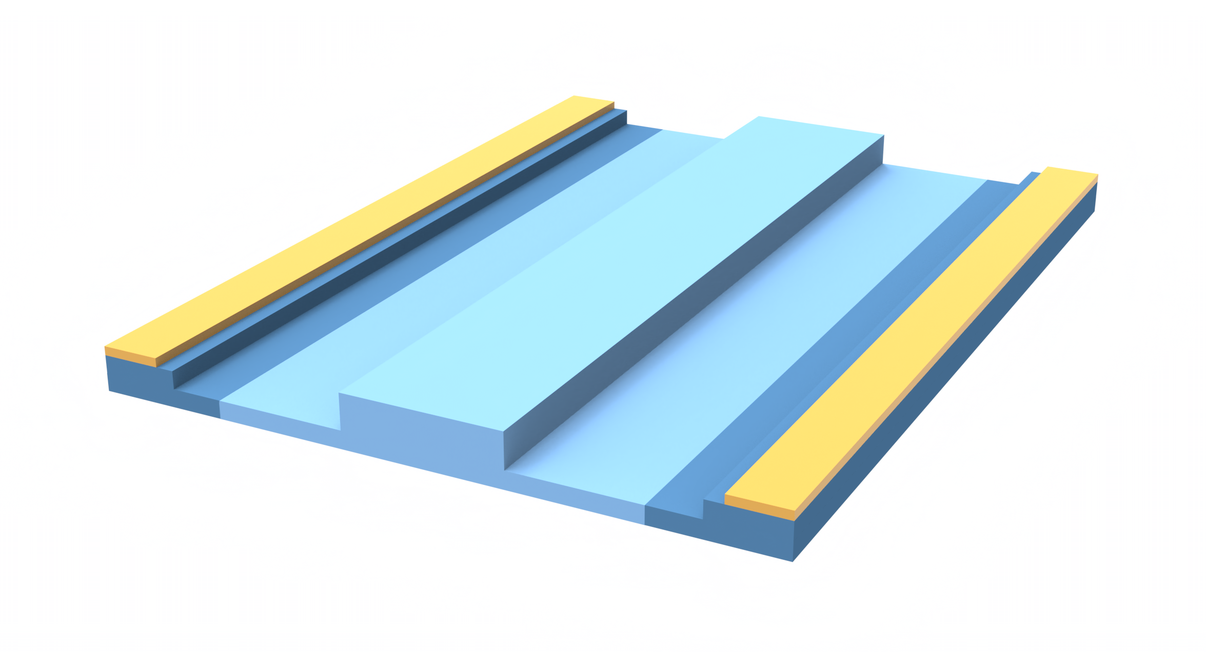
In this example we investigate the modulation of a silicon waveguide with an embedded doped silicon p++ - p - p++ junction inspired by the design presented in Chuyu Zhong, Hui Ma, Chunlei Sun, Maoliang Wei, Yuting Ye, Bo Tang, Peng Zhang, Ruonan Liu, Junying Li, Lan Li, and Hongtao Lin, "Fast thermo-optical modulators with doped-silicon heaters operating at 2 μm", Opt. Express 29, 23508-23516 (2021). The primary modulation effect is due to heating occurring inside the waveguide as a potential difference is applied across the p++ - p - p++ junction. For calculation of current flowing through the device we use our Charge solver. The non-isothermal analysis option allows the solver to also provide the temperature distribution from both Joule heating and generation/recombination heat sink/source.
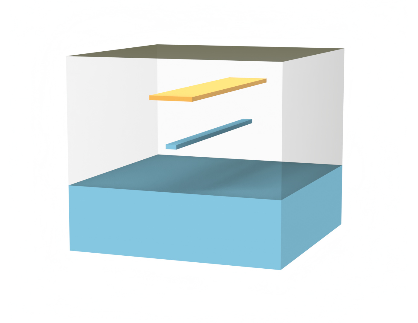
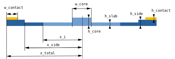
The sketch below highlights the geometric features of the considered waveguide:
We begin by importing the required modules for this example.
import numpy as np
import tidy3d as td
import tidy3d.web as web
from matplotlib import pyplot as plt
from tidy3d.log import log
Next, let's define some geometric properties of the waveguide as well as the doping. We define three doping regions within the Si waveguide with concentrations p++ - p - p++. The interface between the high doping concentration and low doping concentration is delimited by [-x_i, x_i] with $x=0$ being the center of the waveguide.
# modulator cross section parameters (µm)
w_core = 0.5
h_core = 0.34
h_slab = 0.1
h_side = 0.1
w_contact = 0.5
x_side = 2.25
x_total = 3
x_i = 1.75
h_contact = 0.05
# for the present setup this contact height is not relevant
# since the conductors are not included in the simulation

# modulator doping concentrations (1/cm^3)
conc_p = 3.5e17
conc_pp = 0.85e20
Let's now define some reference temperature and wavelength:
Tref = 300
wvl_um = 2
freq0 = td.C_0 / wvl_um
We define next dimensions for the cladding and buried oxide box:
# cladding dimensions (µm)
sim_width = 20
h_cladding = 2  # thickness of cladding
h_box = 1.5  # thickness of buried oxide

# define center of the cladding so that the device sits 2um above
center_cladding = (0, h_cladding / 2, 0)
center_box = (0, -h_box / 2, 0)
center_sim = (0, (h_cladding - h_box) / 2, 0)
Next we define some optical and thermal properties for Si and SiO2. Thermal properties can be extracted from www.efunda.com, www.periodic-table.org and www.azom.com
# Si properties
Si_dndT = 1.76e-4  # Si thermo-optic coefficient dn/dT, 1/K

Si_k = 148e-6  # Si thermal conductivity, W / (um * K)
Si_s = 710  # Si specific heat capacity, J / (Kg * K)

# SiO2 properties
SiO2_n = 1.444  # SiO2 refraction index
SiO2_dndT = 1e-5  # SiO2 thermo-optic coefficient dn/dT, 1/K

SiO2_k = 1.38e-6  # SiO2 thermal conductivity, W/(um*K)
SiO2_s = 709  # SiO2 specific heat capacity, J / (Kg * K)\
Heat-Charge simulation
We will begin by creating a HeatChargeSimulation object. To define it we will need to create at least one SemiconductorMedium. For this type of medium we can define the doping distributions that will be applied to all structures that have this as their medium.
Let's start, then, with creating the doping. There are two main ways of defining doping in Tidy3d: supplying a SpatialDataArray with the desired doping distribution or through doping boxes.
In what follows we'll use doping boxes. One thing to note is that these boxes are additive meaning that regions with boxes overlap will see the sum of the doping corresponding to each of the boxes.
Additionally, there are different types of doping boxes. Here we'll be using ConstantDoping and GaussianDoping. Gaussian doping allow for smooth transition of one doping level to another.
acceptors = []

acceptors.append(
    td.ConstantDoping(
        center=[0, 0, 0], size=[2 * x_total, 2 * h_core, td.inf], concentration=conc_p
    )
)

acceptors.append(
    td.GaussianDoping.from_bounds(
        rmin=[-x_total, -10 * h_side, -td.inf],
        rmax=[-x_i, 10 * h_side, td.inf],
        concentration=conc_pp - conc_p,
        ref_con=conc_p,
        width=4 * h_side,
        source="xmin",
    )
)

acceptors.append(
    td.GaussianDoping.from_bounds(
        rmin=[x_i, -10 * h_side, -td.inf],
        rmax=[x_total, 10 * h_side, td.inf],
        concentration=conc_pp - conc_p,
        ref_con=conc_p,
        width=4 * h_side,
        source="xmax",
    )
)
Next we'll use this doping to define the semiconductor properties.
You can see how materials are defined with the MultiPhysicsMedium class which allows to define physical group of properties, e.g., optical, thermal, and electrical properties.
The exception is air which is defined as Medium. This is because air structures will be removed from our Heat-Charge simulation.
# let's define a material here for our Charge simulations
si_doped = td.MultiPhysicsMedium(
    optical=td.material_library["cSi"]["Palik_Lossless"],
    charge=td.SemiconductorMedium(
        permittivity=11.1,
        N_c=td.ConstantEffectiveDOS(N=2.86e19),
        N_v=td.ConstantEffectiveDOS(N=3.1e19),
        E_g=td.ConstantEnergyBandGap(eg=1.11),
        mobility_n=td.ConstantMobilityModel(mu=400),
        mobility_p=td.ConstantMobilityModel(mu=200),
        R=[td.ShockleyReedHallRecombination(tau_n=1e-8, tau_p=1e-8)],
        N_a=acceptors,
    ),
    heat=td.SolidMedium(
        conductivity=Si_k,
        capacity=Si_s,
    ),
    name="Si",
)

SiO2 = td.MultiPhysicsMedium(
    optical=td.Medium.from_nk(n=SiO2_n, k=0, freq=freq0),
    heat=td.SolidSpec(conductivity=SiO2_k, capacity=SiO2_s),
    charge=td.ChargeInsulatorMedium(permittivity=SiO2_n**2),
    name="SiO2",
)

air = td.Medium(heat_spec=td.FluidSpec(), name="air")
Structures
We create now all the structures used in both the optic and Heat-Charge simulations.
core = td.Structure(
    geometry=td.Box(center=(0, h_core / 2, 0), size=(w_core, h_core, td.inf)),
    medium=si_doped,
    name="core",
)

left_slab = td.Structure(
    geometry=td.Box(
        center=(-(x_side + w_core / 2) / 2, h_slab / 2, 0),
        size=(x_side - w_core / 2, h_slab, td.inf),
    ),
    medium=si_doped,
    name="left_slab",
)

left_side = td.Structure(
    geometry=td.Box(
        center=(-(x_side + x_total) / 2, h_side / 2, 0), size=(x_total - x_side, h_side, td.inf)
    ),
    medium=si_doped,
    name="left_side",
)

right_slab = td.Structure(
    geometry=td.Box(
        center=((x_side + w_core / 2) / 2, h_slab / 2, 0),
        size=(x_side - w_core / 2, h_slab, td.inf),
    ),
    medium=si_doped,
    name="right_slab",
)

right_side = td.Structure(
    geometry=td.Box(
        center=((x_side + x_total) / 2, h_side / 2, 0), size=(x_total - x_side, h_side, td.inf)
    ),
    medium=si_doped,
    name="right_side",
)

cladding = td.Structure(
    geometry=td.Box(center=center_sim, size=(sim_width, h_cladding + h_box, td.inf)),
    medium=SiO2,
    name="cladding",
)

# create objects for heat simulation
substrate = td.Structure(
    geometry=td.Box(center=(0, -h_box - h_slab / 2, 0), size=(sim_width, h_slab, td.inf)),
    medium=si_doped,
    name="substrate",
)
For ease in defining boundary conditions we define here some auxiliary structures made up of a conductive medium defined with ChargeConductorMedium
contact_medium = td.MultiPhysicsMedium(
    charge=td.ChargeConductorMedium(conductivity=1), name="contact"
)

contact_p = td.Structure(
    geometry=td.Box(
        center=(-x_total + w_contact / 2, h_side + h_contact / 2, 0),
        size=(w_contact, h_contact, td.inf),
    ),
    medium=contact_medium,
    name="contact_p",
)

contact_n = td.Structure(
    geometry=td.Box(
        center=(x_total - w_contact / 2, h_side + h_contact / 2, 0),
        size=(w_contact, h_contact, td.inf),
    ),
    medium=contact_medium,
    name="contact_n",
)
Scene
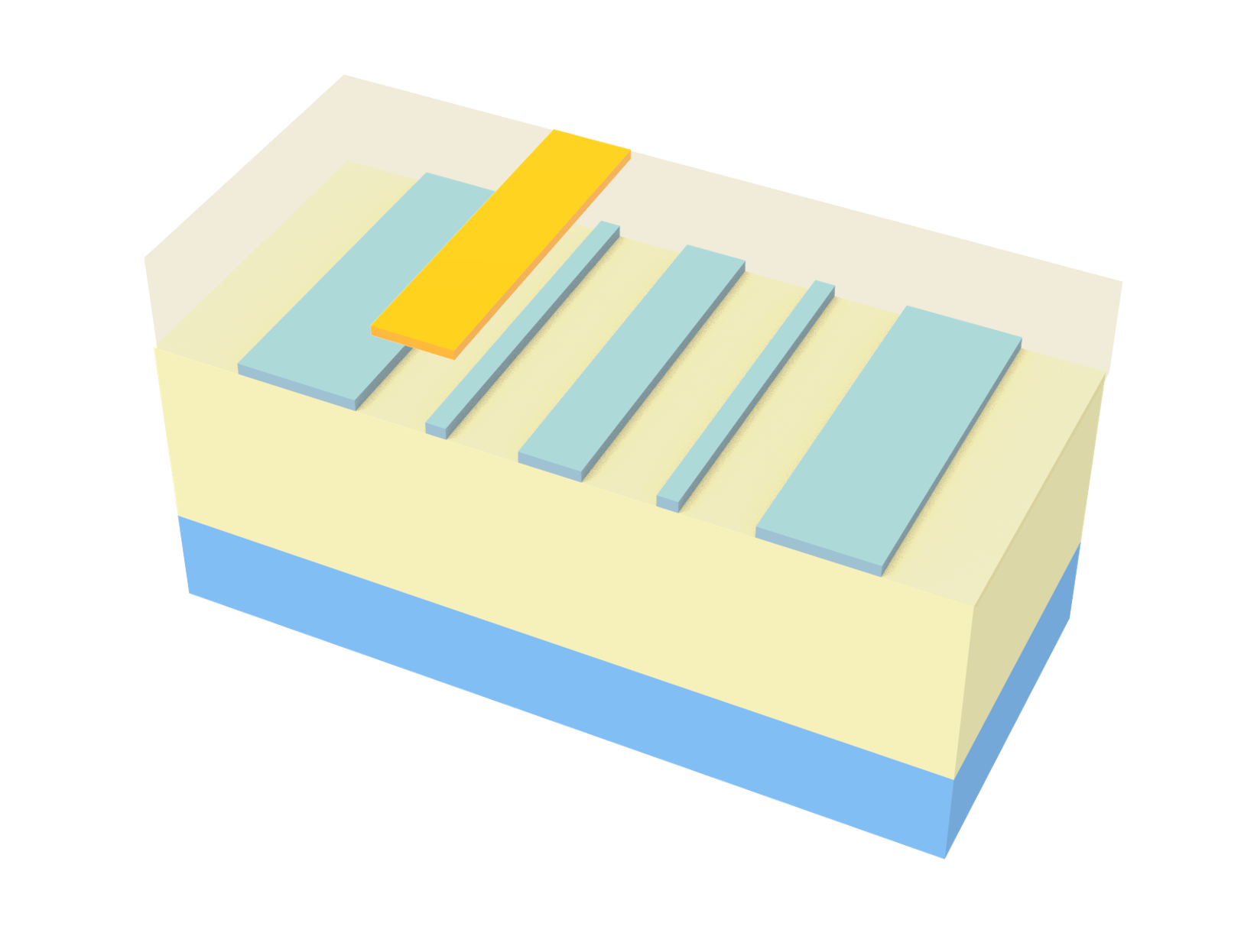
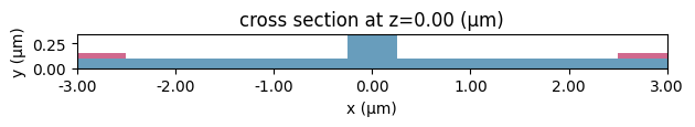
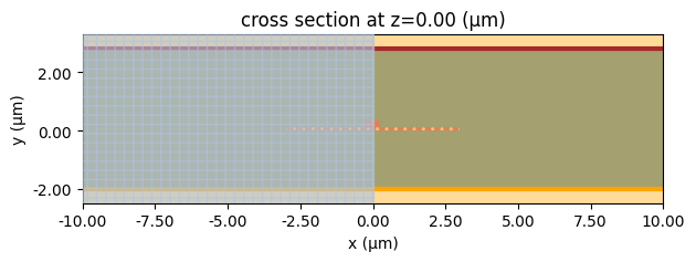
We can now put those structures together into a scene and explore what it looks like
# create a scene with the previous structures
Si_structures = [left_side, left_slab, core, right_slab, right_side]

all_structures = [cladding, substrate] + Si_structures + [contact_p, contact_n]

scene_charge = td.Scene(
    medium=air,
    structures=all_structures,
)

scene_charge.plot(z=0)
plt.show()
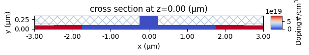
Let's also inspect the doping profiles and make sure it is what we were expecting. Note the smooth transition of doping between the p and p+ regions. These smooth transitions avoid sharp variations in electric potential hence avoiding artificially high electric field. This is relevant in non-isothermal simulations since some of the heat source terms are proportional to the electric field.
ax = scene_charge.plot_structures_property(z=0, property="doping")
ax.set_xlim(-x_total, x_total)
plt.show()
Boundary conditions
Since we're interested in the response of the system for different applied voltages we'll need to solve the Heat-Charge problem at each of these voltages.
First we deal with electric boundary conditions. For this case we apply VoltageBC to both conductors. This BC requires the definition of a source. We'll be using DCVoltageSource which can accept and array of voltages. When an array is provided a parameter scan will be run and the returned data will have the provided voltage values as a separate dimension.
Let's define forward bias values up to 5 V with a step of 0.5 V.
# create BCs
voltages = np.arange(0.0, 5.0, 0.5)

bc_v1 = td.HeatChargeBoundarySpec(
    condition=td.VoltageBC(source=td.DCVoltageSource(voltage=voltages)),
    placement=td.StructureBoundary(structure=contact_p.name),
)

bc_v2 = td.HeatChargeBoundarySpec(
    condition=td.VoltageBC(source=td.DCVoltageSource(voltage=0)),
    placement=td.StructureBoundary(structure=contact_n.name),
)

boundary_conditions = [bc_v1, bc_v2]
We next create thermal boundary conditions. We define two BCs: a temperature BC applied to the auxiliary Si structure; and convection boundary condition applied to the interface between the mediums air and SiO2.
bc_air = td.HeatChargeBoundarySpec(
    condition=td.ConvectionBC(ambient_temperature=300, transfer_coeff=10 * 1e-12),
    placement=td.MediumMediumInterface(mediums=[air.name, SiO2.name]),
)

bc_substrate = td.HeatChargeBoundarySpec(
    condition=td.TemperatureBC(temperature=300),
    placement=td.StructureStructureInterface(structures=[substrate.name, cladding.name]),
)

heat_bc = [bc_air, bc_substrate]
Monitors
Since we're interested in obtaining the free carrier distribution we'll add a SteadyFreeCarrierMonitor to our Charge simulation. For visualization purposes we will also include a potential monitor, i.e., SteadyPotentialMonitor
Note that the below monitors have been defined with infinite size to cover the full domain. This will be later helpful when we interpolate carrier and temperature data onto the optics simulation domain.
charge_mnt = td.SteadyFreeCarrierMonitor(
    center=(0, 0, 0),
    size=(td.inf, td.inf, td.inf),
    name="charge_mnt",
    unstructured=True,
)

potential_mnt = td.SteadyPotentialMonitor(
    center=(0, 0, 0),
    size=(td.inf, td.inf, td.inf),
    name="potential_mnt",
    unstructured=True,
)
charge_monitors = [charge_mnt, potential_mnt]
Since we're also interested in the temperature field we need to define a temperature monitor:
# set a temperature monitor
temp_mnt = td.TemperatureMonitor(
    center=(0, 0, 0),
    size=(td.inf, td.inf, td.inf),
    name="temperature",
    unstructured=True,
)
Heat-Charge simulation object
When running Charge, we need to define the type of Charge simulation and some convergence settings. In the current case we set a relative tolerance of $1\cdot 10^{-5}$ and an absolute tolerance of $5\cdot 10^{10}$. The absolute tolerance may seem big though one should notice we have variables (electrons/holes) that take on values many orders of magnitude larger than the tolerance ($\approx 10^{20}$).
In the current case, we are going to run a non isothermal DC case which we can define the simulation with SteadyChargeDCAnalysis. In DC mode we can set the parameter convergence_dv which tells the solver to limit the size of the sweep, i.e., if we need to solve for a bias of 0 and 0.5 and we set convergence_dv=0.1, it will force the solver to go between 0 and 0.5 at intervals of 0.1.
convergence_settings = td.ChargeToleranceSpec(
    rel_tol=1e-5, abs_tol=1e10, max_iters=200, ramp_up_iters=2
)

analysis_type = td.SteadyChargeDCAnalysis(
    tolerance_settings=convergence_settings, convergence_dv=0.5
)
The last element we need to define before we can run the heat simulation is the mesh which we build using Tidy3D function DistanceUnstructuredGrid().
We will give this function 5 arguments:
-
dl_interfacedefines the grid size near the interface. -
dl_bulkdefines the grid size away from the interface. -
distance_interfacedefines the distance from the interface until whichdl_interfacewill be enforced. -
distance_bulkdefines the distance from the interface after whichdl_bulkwill be enforced. -
non_refined_structuresallows us to specify structures which will not be refined. -
mesh_refinementsallows us to specify an array of refinement regions.
We'll use a spatial resolution of $0.005\mu m$ to refine the semiconductor region.
res = 0.005
dl_min = h_slab / 3
dl_max = 10 * dl_min

refinement_region = td.GridRefinementRegion(
    size=(2 * x_total, h_core, 0),
    center=(0, h_core / 2, 0),
    dl_internal=res,
    transition_thickness=res * 10,
)

mesh = td.DistanceUnstructuredGrid(
    dl_interface=dl_min,
    dl_bulk=dl_max,
    distance_interface=dl_min,
    distance_bulk=4 * dl_max,
    non_refined_structures=[substrate.name],  # do not refine near wafer
    mesh_refinements=[refinement_region],
)
We now have all the required elements to define a Charge simulation object. Note that the simulation has 0 size in the $z$ direction. With this, we'll make sure that the simulation is 2D even if the structures themselves are not.
# build heat simulation object
charge_sim = td.HeatChargeSimulation.from_scene(
    scene=scene_charge,
    monitors=charge_monitors + [temp_mnt],
    analysis_spec=analysis_type,
    center=center_sim,
    size=(sim_width, h_cladding + h_box + 1, 0),
    boundary_spec=boundary_conditions + heat_bc,
    grid_spec=mesh,
)
15:31:59 CET WARNING: Structure at 'structures[0]' has bounds that extend
             exactly to simulation edges. This can cause unexpected behavior. If
             intending to extend the structure to infinity along one dimension,
             use td.inf as a size variable instead to make this explicit.
WARNING: Suppressed 3 WARNING messages.
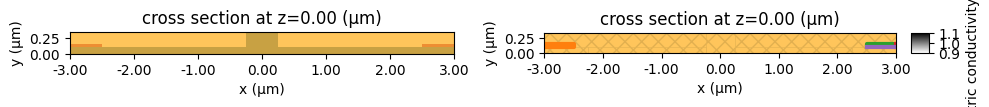
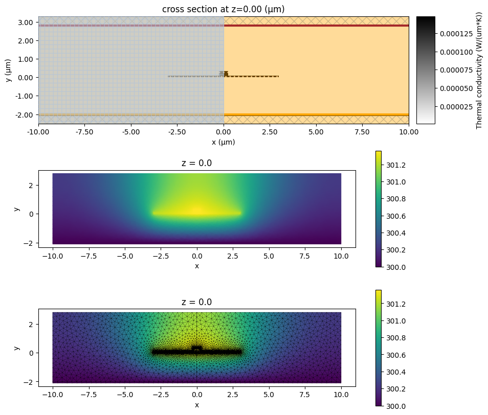
Next let's visualize our simulation domain. In the upper plot we visualize the domain with the thermal conductivity superimposed to the structures. It can be seen that the semiconductor region has higher (darker) thermal conductivity. The boundary conditions can also be seen: the red line indicates the convection BC whereas the yellow line at the bottom indicates the temperature BC.
The plot at the bottom shows the simulation structures of the Charge simulation along with the voltage BCs highlighted with a yellow line.
fig, ax = plt.subplots(2, 1, figsize=(10, 5))
charge_sim.plot_property(z=0, property="heat_conductivity", monitor_alpha=0, ax=ax[0])
charge_sim.plot(z=0, monitor_alpha=0, ax=ax[1])
ax[1].set_xlim(-x_total, x_total)
ax[1].set_ylim(-h_core, h_core)
plt.tight_layout()
plt.show()
Now we can run the Charge simulation.
charge_data = web.run(charge_sim, task_name="modulator", path="charge_modulator.hdf5")
15:32:00 CET Created task 'modulator' with resource_id
             'hec-62bd17de-0202-4a23-af5a-c8961fef0d35' and task_type
             'HEAT_CHARGE'.
             Tidy3D's HeatCharge solver is currently in the beta stage. Cost of
             HeatCharge simulations is subject to change in the future.
Output()
15:32:04 CET Estimated FlexCredit cost: 0.025. Minimum cost depends on task
             execution details. Use 'web.real_cost(task_id)' to get the billed
             FlexCredit cost after a simulation run.
15:32:06 CET status = success
Output()
15:32:10 CET Loading simulation from charge_modulator.hdf5
             WARNING: Structure at 'structures[0]' has bounds that extend
             exactly to simulation edges. This can cause unexpected behavior. If
             intending to extend the structure to infinity along one dimension,
             use td.inf as a size variable instead to make this explicit.
WARNING: Suppressed 3 WARNING messages.
             WARNING: Warning messages were found in the solver log. For more
             information, check 'SimulationData.log' or use
             'web.download_log(task_id)'.
Solution visualization
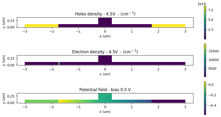
We can begin by examining the electron, hole, and potential distributions at a couple of applied biases:
_, ax = plt.subplots(3, 1, figsize=(10, 5))

np.log10(charge_data["charge_mnt"].holes.sel(z=0, voltage=voltages[-1])).plot(grid=False, ax=ax[0])
ax[0].set_title(f"Holes density - {voltages[-1]}V  - (cm$^-$$^3$)")

np.log10(charge_data["charge_mnt"].electrons.sel(z=0, voltage=voltages[-1])).plot(
    grid=False, ax=ax[1], vmax=8
)
ax[1].set_title(f"Electron density - {voltages[-1]}V  - (cm$^-$$^3$)")

for ind in range(2):
    ax[ind].set_xlabel("x (um)")
    ax[ind].set_ylabel("y (um)")

ax[2] = (
    charge_data["potential_mnt"]
    .potential.sel(z=0, voltage=voltages[1])
    .plot(grid=False, ax=ax[2], vmax=0.0)
)
ax[2].set_title(f"Potential field - bias {voltages[1]:1.1f} V")
ax[2].set_xlabel("x (um)")
ax[2].set_ylabel("y (um)")

for ind in range(3):
    ax[ind].set_xlim(-x_total, x_total)
    ax[ind].set_ylim(0, h_core)

plt.tight_layout()
plt.show()
/home/marc/Documents/tidy3D_python/tidy3d_local/lib/python3.12/site-packages/xarray/computation/apply_ufunc.py:818: RuntimeWarning: divide by zero encountered in log10
  result_data = func(*input_data)
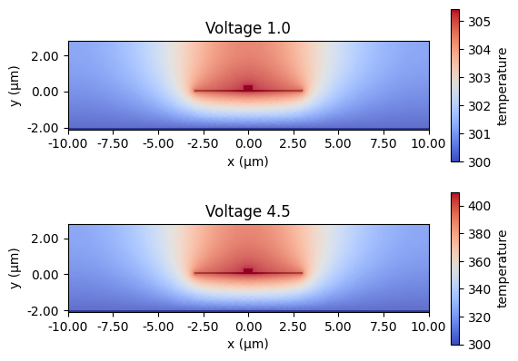
We can also explore the temperature field at two different applied biases:
_, ax = plt.subplots(2, 1, figsize=(10, 5))
charge_data["temperature"].temperature.sel(z=0, voltage=1).plot(ax=ax[0], grid=False)
charge_data["temperature"].temperature.sel(z=0, voltage=4.5).plot(ax=ax[1], grid=False)
plt.show()
We can further inspect how electrons and holes as well as the potential vary across the semiconductor at different biases by plotting the distribution along the coordinate $y=h\_side/2$:
_, ax = plt.subplots(1, 3, figsize=(10, 4))
for v in range(5):
    electrons = charge_data["charge_mnt"].electrons.sel(y=h_side / 2, z=0, voltage=v)
    x_vals = electrons.coords.get("x").values
    e_vals = np.squeeze(electrons.values)
    ax[0].semilogy(x_vals, e_vals, label=f"v={v}V")
    ax[0].set_xlim(-x_total, x_total)

    holes = charge_data["charge_mnt"].holes.sel(y=h_side / 2, z=0, voltage=v)
    x_vals = holes.coords.get("x").values
    h_vals = np.squeeze(holes.values)
    ax[1].semilogy(x_vals, h_vals, label=f"v={v}V")
    ax[1].set_xlim(-x_total, x_total)

    potential = charge_data["potential_mnt"].potential.sel(y=h_side / 2, z=0, voltage=v)
    x_vals = potential.coords.get("x").values
    p_vals = np.squeeze(potential.values)
    ax[2].plot(x_vals, p_vals, label=f"v={v}V")
    ax[2].set_xlim(-x_total, x_total)

for ax_ind in range(3):
    ax[ax_ind].legend()
    ax[ax_ind].set_xlabel("x (um)")

ax[0].set_ylabel("Electron Concentration (cm$^{-3}$)")
ax[1].set_ylabel("Hole Concentration (cm$^{-3}$)")
ax[2].set_ylabel("Potential (V)")
plt.tight_layout()
plt.show()
As it can be seen the majority carrier (holes) is dominated by the doping profile wheres the minority carrier (electrons) clearly changes with the different applied voltages. The potential varies roughly linearly along $x$ as a result of the hole concentration following the doping concentration.
Similarly, we can check the temperature distribution along $y=h\_side/2$
for v in range(5):
    temp = charge_data["temperature"].temperature.sel(y=h_side / 2, z=0, voltage=v)
    x_vals = temp.coords.get("x").values
    t_vals = np.squeeze(temp.values)
    plt.plot(x_vals, t_vals, label=f"v={v}V")
plt.xlabel("x (um)")
plt.ylabel("Temperature (K)")
plt.legend()
plt.show()
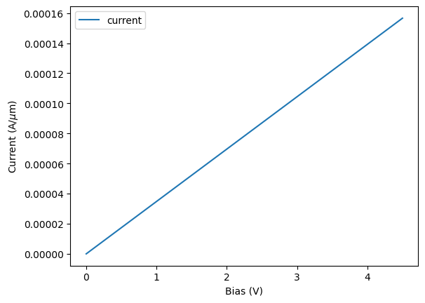
Whenever we run a charge simulation, Charge will output some device characteristics. These are not linked to any monitor but instead they are related to the whole device. For the current DC isothermal simulation we have the entry steady_dc_current_voltage.
# let's plot the current as a function of the applied voltages
_, ax = plt.subplots(1, 1)
# since this is a 2D simulation the current is provided in A/um
currents = np.abs(charge_data.device_characteristics.steady_dc_current_voltage.values)
ax.plot(voltages, currents, label="current")
ax.set_xlabel("Bias (V)")
ax.set_ylabel(r"Current (A/$\mu$m)")
ax.legend()
plt.show()
Perturbation mediums
We next create perturbation materials. These include the necessary $k$ and $n$ perturbations to account for the effect of both temperature and carrier concentration.
We can create a perturbed medium using PerturbationMedium() of Tidy3D. In this case, the permittivity of Si will change with charge and temperature; and the permittivity of SiO2 will only vary with temperature.
It should be noted that a linear variation with temperature is considered, i.e., the temperature dependence of permittivity with temperature has been linearized at the given reference temperature.
For the Si charge-induced variation, we will use the empirical relationships presented in M. Nedeljkovic, R. Soref and G. Z. Mashanovich, "Free-Carrier Electrorefraction and Electroabsorption Modulation Predictions for Silicon Over the 1–14- μm Infrared Wavelength Range," IEEE Photonics Journal, vol. 3, no. 6, pp. 1171-1180, Dec. 2011 which has been implemented in the class NedeljkovicSorefMashanovich.
Note also that since the permittivity of the material is a function of wave frequency, we require a reference wavelength. A reference temperature must also be given for the same reason.
# Perturbation models for Si
perturbation_model = td.NedeljkovicSorefMashanovich(ref_freq=freq0)

n_si, k_si = si_doped.optical.nk_model(frequency=td.C_0 / wvl_um)
si_non_perturb = td.Medium.from_nk(n=n_si, k=k_si, freq=freq0)

# temperature perturbation
dn_si_heat = td.LinearHeatPerturbation(coeff=Si_dndT, temperature_ref=Tref)

si_perturb = td.PerturbationMedium.from_unperturbed(
    medium=si_non_perturb,
    perturbation_spec=td.IndexPerturbation(
        delta_n=perturbation_model.delta_n().updated_copy(heat=dn_si_heat),
        delta_k=perturbation_model.delta_k(),
        freq=freq0,
    ),
    name="Si_perturbed",
)
The warning above is telling us that the perturbation model does not check whether the perturbed permittivity or conductivity are physical so it is up to us to check that (which we'll do below). Since this message is going to be repeated every time we create a perturbation we will temporarily set the logging level to "ERROR"
td.config.logging_level = "ERROR"
# Perturbation model for SiO2
SiO2_perturbed = td.PerturbationMedium.from_unperturbed(
    medium=SiO2.optical,
    perturbation_spec=td.IndexPerturbation(
        delta_n=td.ParameterPerturbation(
            heat=td.LinearHeatPerturbation(coeff=SiO2_dndT, temperature_ref=Tref)
        ),
        freq=freq0,
    ),
    name="SiO2_perturbed",
)
Combined Electric and Thermal Perturbations
In order to reuse the scene we created for the non isothermal Charge simulation, we need to update the mediums of the structures. This can be done by looping through the structures of the scene and updating the medium accordingly as below.
Note that since the perturbation models can't ensure that the resulting permittivity stays above 1 a warning is issued every time a structure is assigned a perturbed medium.
# recreate scene with perturbation medium
structs_perturbed = []
for n, structure in enumerate(scene_charge.structures):
    if structure.medium.name == "Si":
        structs_perturbed.append(
            structure.updated_copy(medium=si_perturb.updated_copy(name=f"Si_perturbed_{n}"))
        )
    elif structure.medium.name == "SiO2":
        structs_perturbed.append(
            structure.updated_copy(medium=SiO2_perturbed.updated_copy(name=f"SiO2_perturbed_{n}"))
        )
    elif structure.medium.optical is not None:
        structs_perturbed.append(structure.updated_copy(medium=structure.medium.optical))
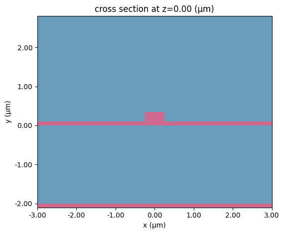
With the structures now having perturbation mediums we can next update the scene and visualize.
with log as consolidated_logger:
    scene_perturbed = scene_charge.updated_copy(structures=structs_perturbed)
    scene_perturbed.plot(z=0)
plt.show()
Before we can apply thermal and carrier perturbations we need to generate a reference optic simulation object:
grid_spec = td.GridSpec.auto(min_steps_per_wvl=50, wavelength=wvl_um)

optic_sim = td.Simulation.from_scene(
    scene=scene_perturbed,
    center=center_sim,
    size=(sim_width, h_cladding + h_box + 1, wvl_um),
    run_time=1e-15,
    grid_spec=grid_spec,
)
Now that we have the reference optical simulation we can create a list of perturbed optical simulations which we can do with perturbed_mediums_copy().
perturbed_sims = []

target_grid = optic_sim.grid.boundaries

for n, v in enumerate(voltages):
    psim = optic_sim.perturbed_mediums_copy(
        electron_density=charge_data["charge_mnt"].electrons.sel(voltage=v),
        hole_density=charge_data["charge_mnt"].holes.sel(voltage=v),
        temperature=charge_data["temperature"].temperature.sel(voltage=v),
    )

    perturbed_sims.append(psim)
We can now verify that all perturbations have the real part of the permittivity greater than 1:
# Check that perturbed permittivity is physical
sample_region = td.Box(
    center=center_sim,
    size=(sim_width, h_cladding + h_box, 0),
)

eps_gt_1 = []
for psim in perturbed_sims:
    eps = psim.epsilon(box=sample_region).isel(z=0, drop=True).data
    eps_gt_1 = eps_gt_1 + (np.real(eps) > 1).tolist()

if all(eps_gt_1):
    print("All perturbed permittivities are greater than 1")
else:
    print("Some perturbed permittivities are not physical!")
All perturbed permittivities are greater than 1
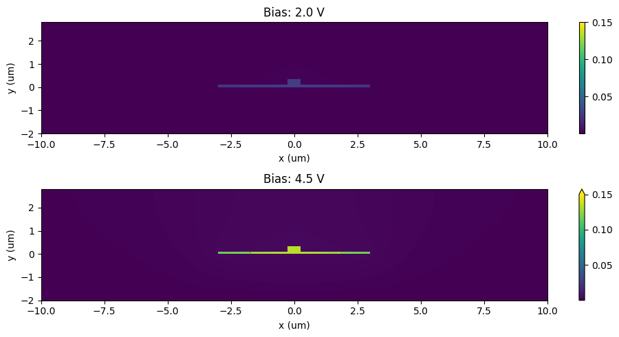
Now that we have created the perturbed simulation we can examine the change in permittivity due to these perturbations:
eps_reference = perturbed_sims[0].epsilon(box=sample_region).isel(z=0, drop=True)

_, ax = plt.subplots(2, 1, figsize=(10, 5))
for ax_ind, n in enumerate([4, 9]):
    eps_doped = perturbed_sims[n].epsilon(box=sample_region).isel(z=0, drop=True)
    eps_doped = eps_doped.interp(x=eps_reference.x, y=eps_reference.y)
    eps_diff = np.abs(np.real(eps_doped - eps_reference))
    eps_diff.plot(x="x", ax=ax[ax_ind], vmax=0.15)

    ax[ax_ind].set_xlabel("x (um)")
    ax[ax_ind].set_ylabel("y (um)")

    ax[ax_ind].set_title(f"Bias: {voltages[n]:1.1f} V")

plt.tight_layout()
plt.show()
Perturbation Mode Analysis
Instead of running a full wave simulation we will compute the modes of the waveguide. This is a smaller computation that will also highlight the influence of the temperature field over the refraction coefficient.
We will compute the waveguide modes on a plane centered around the core section of the device:
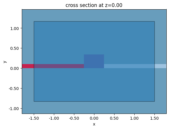
mode_plane = td.Box(center=(0, h_core / 2, 0), size=(3, 2, 0))

fig, ax = plt.subplots(1, 1)
perturbed_sims[0].plot(z=0, ax=ax)
mode_plane.plot(z=0, ax=ax, alpha=0.5)
plt.show()
The next few lines create the mode simulation objects for each of the temperature and carrier fields and submits the computation.
from tidy3d.plugins.mode import ModeSolver

mode_solvers = {}

for n, psim in enumerate(perturbed_sims):
    name = "psim" + str(n)
    mode_solvers[name] = ModeSolver(
        simulation=psim,
        plane=mode_plane,
        mode_spec=td.ModeSpec(num_modes=1, precision="double"),
        freqs=[freq0],
    )
Run all mode solver simulations in a batch.
mode_datas = web.Batch(simulations=mode_solvers, reduce_simulation=True).run()
Output()
15:33:21 CET Started working on Batch containing 10 tasks.
15:33:39 CET Maximum FlexCredit cost: 0.040 for the whole batch.
             Use 'Batch.real_cost()' to get the billed FlexCredit cost after
             completion.
Output()
15:34:04 CET Batch complete.
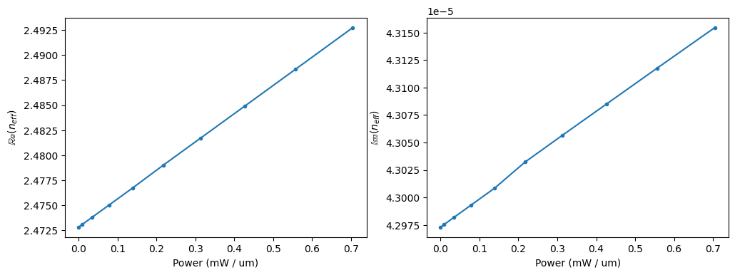
And finally we can see the combined effect of both thermal and carrier density on the refraction index.
In the following we're computing the electric power as $P_{electric}=V \cdot i$. It is reminded here that since the Charge simulation was 2D the current has dimensions of $A/\mu m$.
Also note that we're setting the logging level back to "WARNING".
td.config.logging_level = "WARNING"

n_eff = np.array([md.n_complex.sel(f=freq0, mode_index=0) for md in mode_datas.values()])

power_mw = np.array(voltages) * np.array(currents) * 1e3

# plot n_eff
_, ax = plt.subplots(1, 2, figsize=(10, 4))
ax[0].plot(power_mw, np.real(n_eff), ".-")
ax[0].set_ylabel(r"$\mathbb{Re}(n_{eff}$)")
ax[0].set_xlabel("Power (mW / um)")

ax[1].plot(power_mw, np.imag(n_eff), ".-")
ax[1].set_ylabel(r"$\mathbb{Im}(n_{eff}$)")
ax[1].set_xlabel("Power (mW / um)")
plt.tight_layout()
plt.show()
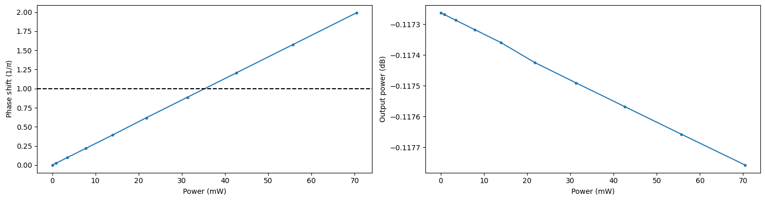
Based on the computed refractive index we can now compute both phase shift and loss over a waveguide length of 100 µm as a function of the input (heating) power. As it can be seen, we'd need to apply a heating power of about $\approx 40mW$ in order to get a phase shift of $\pi$.
wvg_l = 100
phase_shift = 2 * np.pi / wvl_um * (np.real(n_eff) - np.real(n_eff[0])) * wvg_l
intensity = np.exp(-4 * np.pi * np.imag(n_eff) * wvg_l / wvl_um)
power_mw_per_100um = power_mw * 100

_, ax = plt.subplots(1, 2, figsize=(10, 4))
ax[0].plot(power_mw_per_100um, phase_shift / np.pi, ".-")
ax[0].axhline(y=1, color="k", linestyle="--")

ax[0].set_xlabel("Power (mW)")
ax[0].set_ylabel(r"Phase shift ($1/\pi$)")

ax[1].plot(power_mw_per_100um, 10 * np.log10(intensity), ".-")

ax[1].set_xlabel("Power (mW)")
ax[1].set_ylabel("Output power (dB)")

plt.tight_layout()
plt.show()