





import matplotlib.pyplot as plt
import numpy as np
import tidy3d as td
import tidy3d.web as web
from scipy.optimize import brentq
TIDY3D
LEARNING CENTER
Example Library

Self-focusing metamaterial grating coupler
Silicon nitride is an attractive waveguide platform, but its modest index contrast makes surface grating couplers weak: a long grating is needed to radiate all of the guided light. Therefore, the diffracted beam is far wider than the fiber mode and the coupling efficiency is low.
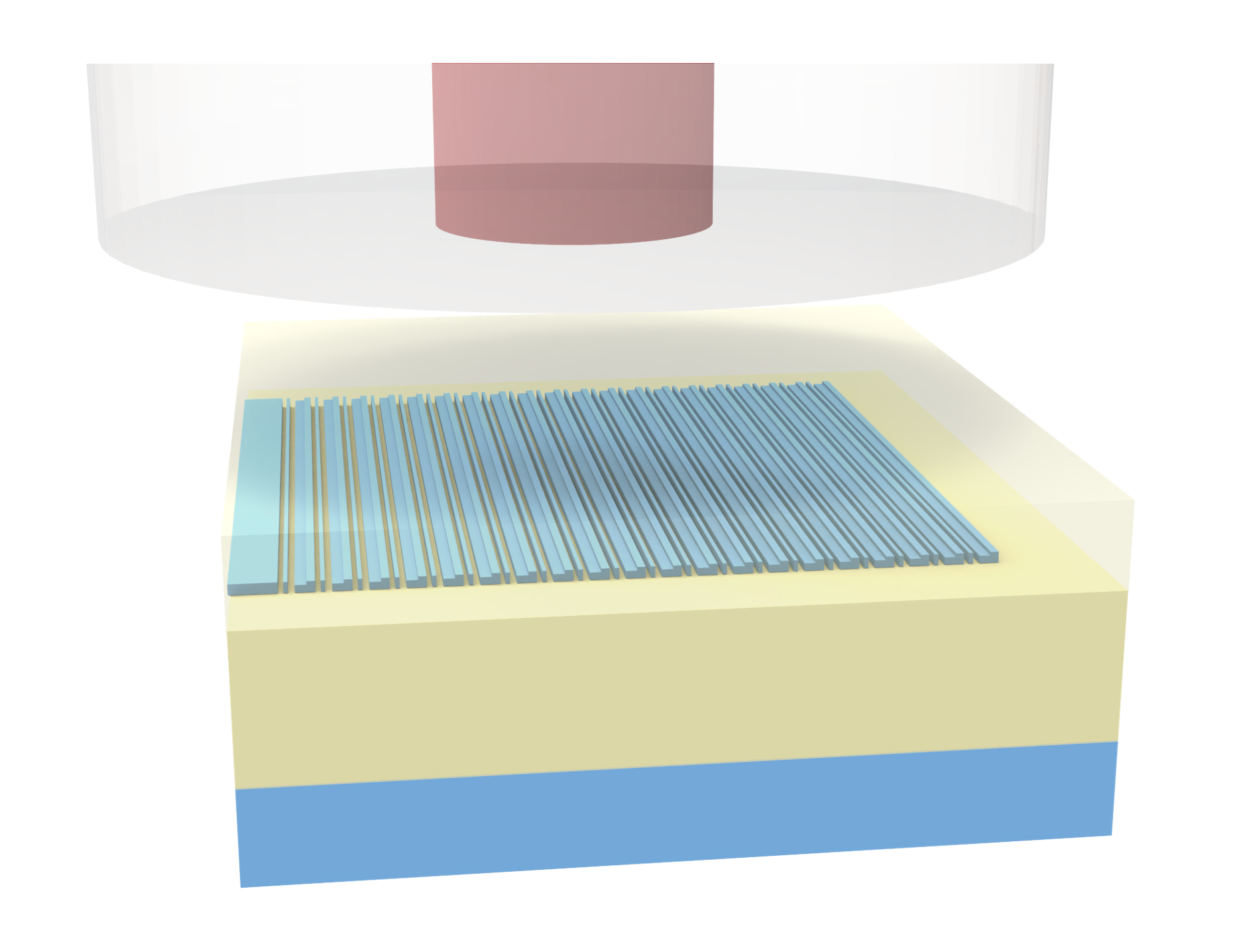
In this notebook, we demonstrate a grating coupler design by combining three mechanisms: a 220 nm amorphous-silicon (\(\alpha\)-Si) overlay that breaks the vertical symmetry and raises the directionality to \(\sim 86\%\); subwavelength metamaterial apodization that shapes a Gaussian near field; and a chirped period that makes the radiated wavefront converge, so a wide near field focuses down onto the fiber mode ~55 \(\mu m\) above the chip. The design is adapted from W. Fraser, D. Benedikovic, R. Korcek, M. Milanizadeh, D.-X. Xu, J. H. Schmid, P. Cheben, and W. N. Ye, “High-efficiency self-focusing metamaterial grating coupler in silicon nitride with amorphous silicon overlay,” Sci. Rep. 14, 11651 (2024).
For more integrated photonic examples, please visit our examples page. If you are new to the finite-difference time-domain (FDTD) method, we highly recommend going through our FDTD101 tutorials.
Simulation Setup
The chip lies in the \(x\)-\(y\) plane and light radiates along \(+z\), with \(z=0\) at the top of the SiN. We cover the O band from 1.27 to 1.35 \(\mu m\). The stack is a 400 nm SiN core on a 4.5 \(\mu m\) buried oxide, carrying a 220 nm \(\alpha\)-Si overlay separated by a 50 nm oxide buffer.
lda0 = 1.31  # central wavelength (um)
freq0 = td.C_0 / lda0
ldas = np.linspace(1.27, 1.35, 9)  # wavelength range of interest (um)
freqs = td.C_0 / ldas
fwidth = 0.5 * (np.max(freqs) - np.min(freqs))

n_sin, n_box, n_buf, n_asi, n_si = 2.0017, 1.4467, 1.4502, 3.5187, 3.5187
h_sin, h_box, h_buf, h_asi = 0.4, 4.5, 0.05, 0.22  # layer thicknesses (um)
w_wg = 0.85  # single-mode SiN feed waveguide width (um)

z_sin = (-h_sin, 0)  # vertical extent of each patterned layer (um)
z_buf = (0, h_buf)
z_asi = (h_buf, h_buf + h_asi)

fiber_h = 55  # fiber height above the chip (um)
mfd = 9.2  # SMF-28 mode field diameter at 1.31 um (um)
The grating itself follows Table 1 of the reference: 13 apodized periods with the pitch chirped from 665 to 639 nm, followed by 27 uniform periods chirped from 638 to 603 nm.
n_apod, n_homo = 13, 27
swg_period = 0.6  # transverse subwavelength period (um)
swg_n_lo = 1.45  # metamaterial index of the weakest tooth
duty = 0.28  # unetched alpha-Si fraction of each period
x_tip, x_g0 = -14.5, -5.8  # waveguide tip and on-axis grating start (um)
fan_half = np.deg2rad(29)  # half opening angle of the SiN sector
min_feature = 0.12  # smallest drawable feature, set by deep-UV lithography (um)

mode_spec = td.ModeSpec(num_modes=1, target_neff=n_sin)  # fundamental TE mode of the feed wire
Slab modes
Three cross-sections matter: the bare SiN slab (the grating trenches), the same slab loaded with the \(\alpha\)-Si overlay (the teeth), and the feed waveguide whose mode we launch. One ModeSimulation helper solves all three locally.
def layer(zc: float, t: float, n: float, w: float = td.inf) -> td.Structure:
    """Return a layer of thickness t and width w, centered at height zc."""
    return td.Structure(geometry=td.Box(center=(0, 0, zc), size=(td.inf, w, t)),
                        medium=td.Medium(permittivity=n**2))


def te0_neff(structures: list, target: float) -> float:
    """Solve the TE0 effective index of a cross-section locally."""
    sim = td.Simulation(
        size=(1, 6, 5), center=(0, 0, -0.6), structures=structures, run_time=1e-13,
        grid_spec=td.GridSpec.auto(min_steps_per_wvl=40, wavelength=lda0),
        boundary_spec=td.BoundarySpec.all_sides(boundary=td.PML()),
    )
    modes = td.ModeSimulation.from_simulation(
        simulation=sim, plane=td.Box(center=(0, 0, -0.6), size=(0, 6, 5)),
        mode_spec=td.ModeSpec(num_modes=1, target_neff=target), freqs=[freq0],
    ).run_local().modes
    return float(np.real(modes.n_eff.values.ravel()[0]))


box, buf = layer(-h_sin - h_box / 2, h_box, n_box), layer(h_buf / 2, h_buf, n_buf)
n_slab = te0_neff([box, layer(-h_sin / 2, h_sin, n_sin), buf], n_sin)
n_tooth = te0_neff([box, layer(-h_sin / 2, h_sin, n_sin), buf,
                    layer(h_buf + h_asi / 2, h_asi, n_asi)], n_asi)
n_wg = te0_neff([box, layer(-h_sin / 2, h_sin, n_sin, w_wg), buf], n_sin)
print(f"bare SiN slab      n_eff = {n_slab:.4f}")
print(f"alpha-Si loaded    n_eff = {n_tooth:.4f}")
print(f"feed waveguide TE0 n_eff = {n_wg:.4f}")
bare SiN slab n_eff = 1.7739
alpha-Si loaded n_eff = 3.0008
feed waveguide TE0 n_eff = 1.6339Metamaterial apodization
Each apodized tooth is a row of \(\alpha\)-Si blocks of width \(w\) on a transverse period \(\Lambda = 600\) nm. Second-order Rytov theory gives the index synthesized by that row, and inverting it converts a target index into a drawable block width. Ramping the index from 1.45 to \(n_{\alpha\text{-}Si}\) over the first 13 periods ramps the grating strength gently, which is what shapes a Gaussian near field. Note that the second-order expansion assumes \(\Lambda \ll \lambda\), and here \(\Lambda/\lambda = 0.46\). The second-order term is therefore not a small correction: it adds 18% at the first period and 77% at the last apodized one, and the resulting curve is non-monotonic, peaking above \(n_{\alpha\text{-}Si}\) at a duty cycle of 0.92. We invert it only on its rising branch, and treat the synthesized indices as a starting point rather than a converged answer.
def emt_index(w: float) -> float:
    """Second-order Rytov index for E perpendicular to the subwavelength interfaces."""
    f = w / swg_period
    par = f * n_asi**2 + (1 - f)
    perp = 1 / (f / n_asi**2 + (1 - f))
    corr = (
        (np.pi**2 / 3)
        * (swg_period / lda0) ** 2
        * f**2
        * (1 - f) ** 2
        * (1 - n_asi**2) ** 2
        * par
        * (perp / n_asi**2) ** 2
    )
    return np.sqrt(perp * (1 + corr))


# emt_index is non-monotonic: it peaks then falls back, so the inversion is only
# single-valued on the rising branch and brentq must be bracketed there.
_scan = np.linspace(1e-4, swg_period, 2001)
w_peak = _scan[np.argmax([emt_index(w) for w in _scan])]


def emt_width(n_target: float) -> float:
    """Invert the effective medium theory on its rising branch."""
    if n_target >= emt_index(swg_period) - 1e-9:
        return swg_period
    return brentq(lambda w: emt_index(w) - n_target, 1e-4, w_peak)


widths = np.linspace(0.01, swg_period, 200)
plt.plot(widths / swg_period, [emt_index(w) for w in widths], c="crimson", label="second order")
plt.plot(widths / swg_period, [np.sqrt(1 / (w / swg_period / n_asi**2 + 1 - w / swg_period)) for w in widths],
         "--", c="gray", label="zeroth order")
plt.axhline(n_asi, c="k", lw=0.8, ls=":")
plt.xlabel("Duty cycle $w/\\Lambda$")
plt.ylabel("Synthesized index")
plt.legend()
plt.grid(alpha=0.3)
plt.show()
pitch = np.concatenate([np.linspace(0.665, 0.639, n_apod), np.linspace(0.638, 0.603, n_homo)])
n_swg = np.concatenate([np.linspace(swg_n_lo, n_asi, n_apod), np.full(n_homo, n_asi)])
block_w = np.array([emt_width(n) for n in n_swg])
x_start = x_g0 + np.concatenate([[0], np.cumsum(pitch)])[:-1]
tooth_len = duty * pitch

print(f"grating length  = {np.sum(pitch):.2f} um")
print(f"gaps close from {(swg_period - block_w[0]) * 1e3:.0f} nm to {(swg_period - block_w[n_apod - 2]) * 1e3:.0f} nm")
grating length = 25.23 um
gaps close from 377 nm to 130 nmFocusing grating lines
The feed waveguide opens into a slab sector, so the in-plane wavefront is cylindrical. Each grating line is placed so that the optical path from the waveguide tip \(O\) to a common point \(F\) is equal along its whole length, \(n_g|OP| + |PF| = \text{const}\). Solving that for every azimuth turns the fan of arcs into a lens.
n_g, focus = 1.81, (-10.1, 110)  # in-plane index and equal-path point (um)
phi = np.linspace(-fan_half, fan_half, 481)


def grating_line(x_axis: float, ph: np.ndarray = None) -> tuple:
    """Return the (x, y) curve whose optical path from tip to focus is constant."""
    ph = phi if ph is None else ph
    xf, zf = focus
    const = n_g * (x_axis - x_tip) + np.hypot(x_axis - xf, zf)

    def residual(r, c, s):
        return n_g * r + np.sqrt((x_tip + r * c - xf) ** 2 + zf**2 + (r * s) ** 2) - const

    r = np.array([brentq(residual, 1e-3, 500, args=(np.cos(a), np.sin(a))) for a in ph])
    return x_tip + r * np.cos(ph), r * np.sin(ph)


def tooth(i: int) -> list:
    """Return the polygon(s) of grating period i, segmented if the period is apodized."""
    lead, trail = x_start[i], x_start[i] + tooth_len[i]
    xl, yl = grating_line(lead)
    if block_w[i] >= swg_period:  # uniform period: one solid arc
        xt, yt = grating_line(trail)
        return [list(zip(xl, yl)) + list(zip(xt[::-1], yt[::-1]))]

    s = np.concatenate([[0], np.cumsum(np.hypot(np.diff(xl), np.diff(yl)))])
    s -= np.interp(0, yl, s)  # arc length measured from the symmetry plane
    polys = []
    for m in range(int(s[0] / swg_period) - 1, int(s[-1] / swg_period) + 2):
        a = max(m * swg_period - block_w[i] / 2, s[0])
        b = min(m * swg_period + block_w[i] / 2, s[-1])
        if b - a <= min_feature:  # drop sub-resolution slivers at the sector edge
            continue
        ph = np.concatenate([[np.interp(a, s, phi)], phi[(s > a) & (s < b)], [np.interp(b, s, phi)]])
        x1, y1 = grating_line(lead, ph)
        x2, y2 = grating_line(trail, ph)
        polys.append(list(zip(x1, y1)) + list(zip(x2[::-1], y2[::-1])))
    return polys


teeth = [poly for i in range(len(pitch)) for poly in tooth(i)]
print(f"{len(teeth)} alpha-Si polygons over {len(pitch)} periods")
280 alpha-Si polygons over 40 periodsfor poly in teeth:
v = np.array(poly)
plt.fill(v[:, 0], v[:, 1], c="teal")
plt.xlabel("x ($\\mu m$)")
plt.ylabel("y ($\\mu m$)")
plt.gca().set_aspect("equal")
plt.show()
Structures
The buffer oxide is a conformal deposition. It rides on the SiN where the mesa exists and drops onto the buried oxide where the SiN has been etched away.
r_out = 1.5 + max(np.hypot(np.array(t)[:, 0] - x_tip, np.array(t)[:, 1]).max() for t in teeth)
sector = [(x_tip, 0)] + [(x_tip + r_out * np.cos(p), r_out * np.sin(p)) for p in phi]
x_join = x_tip + (w_wg / 2) / np.tan(fan_half)
wire_bounds = ((-26, -w_wg / 2), (x_join, w_wg / 2))

sin_medium = td.Medium(permittivity=n_sin**2)
buf_medium = td.Medium(permittivity=n_buf**2)


structures = [
    layer(-h_sin - h_box - 2, 4, n_si),
    layer(-h_sin - h_box / 2, h_box, n_box),
    layer(z_sin[0] + h_buf / 2, h_buf, n_buf),  # buffer on the bare buried oxide
    td.Structure(
        geometry=td.Box.from_bounds((*wire_bounds[0], z_sin[0]), (*wire_bounds[1], z_sin[1])), medium=sin_medium
    ),
    td.Structure(geometry=td.PolySlab(vertices=sector, axis=2, slab_bounds=z_sin), medium=sin_medium),
    td.Structure(
        geometry=td.GeometryGroup(
            geometries=[
                td.Box.from_bounds((*wire_bounds[0], z_buf[0]), (*wire_bounds[1], z_buf[1])),
                td.PolySlab(vertices=sector, axis=2, slab_bounds=z_buf),
            ]
        ),
        medium=buf_medium,
    ),
    td.Structure(
        geometry=td.GeometryGroup(
            geometries=[td.PolySlab(vertices=t, axis=2, slab_bounds=z_asi) for t in teeth]
        ),
        medium=td.Medium(permittivity=n_asi**2),
    ),
]
Source and Monitors
A ModeSource launches the fundamental TE mode into the feed waveguide. A pair of FluxMonitor planes above and below the chip give the directionality, and a ModeMonitor records the back-reflection.
Both field maps come from FieldProjectionCartesianMonitor, which propagates the near field to a plane outside the simulation domain. One projects to the fiber plane 55 \(\mu m\) above the chip (proj_axis=2) for the coupling efficiency; the other projects onto the longitudinal \(x\)-\(z\) cross-section (proj_axis=1) to visualize the beam. We set far_field_approx=False because a 41.6 \(\times\) 35.6 \(\mu m\) aperture at 55 \(\mu m\) sits deep in the Fresnel regime (Fresnel number \(\approx 4.5\)).
x_lo, x_hi, y_half, z_top, z_bot = -21, 23, 19, 3, -h_sin - h_box - 1.6
z_mon, x_src = 1.5, -18.5  # near-field plane and source position (um)
x_c, x_w, y_w = (x_lo + x_hi) / 2, x_hi - x_lo - 2.4, 2 * y_half - 2.4

mode_source = td.ModeSource(
    center=(x_src, 0, -h_sin / 2),
    size=(0, 4, 4),
    source_time=td.GaussianPulse(freq0=freq0, fwidth=fwidth),
    direction="+",
    mode_spec=mode_spec,
)

monitors = [
    td.FluxMonitor(center=(x_c, 0, z_mon), size=(x_w, y_w, 0), freqs=freqs, name="up"),
    td.FluxMonitor(center=(x_c, 0, z_bot + 1), size=(x_w, y_w, 0), freqs=freqs, name="down"),
    td.ModeMonitor(center=(-17, 0, -h_sin / 2), size=(0, 4, 4), freqs=freqs, mode_spec=mode_spec, name="refl"),
    td.FieldProjectionCartesianMonitor(
        center=(x_c, 0, z_mon),
        size=(x_w, y_w, 0),
        freqs=freqs,
        name="fiber_plane",
        proj_axis=2,
        proj_distance=fiber_h - z_mon,
        x=np.linspace(-28, 28, 225),
        y=np.linspace(-28, 28, 225),
        far_field_approx=False,
        interval_space=(3, 3, 1),
    ),
    td.FieldProjectionCartesianMonitor(
        center=(x_c, 0, z_mon),
        size=(x_w, y_w, 0),
        freqs=[freq0],
        name="cross_section",
        proj_axis=1,
        proj_distance=0,
        x=np.linspace(-26, 20, 181),
        y=np.linspace(2, 68, 141),
        far_field_approx=False,
        interval_space=(3, 3, 1),
    ),
]
We now assemble the Simulation. A MeshOverrideStructure refines the vertical grid across the thin layer stack, where the 50 nm buffer oxide is the binding feature. It does not change the in-plane grid: the silicon handle wafer is unbounded in \(x\) and \(y\), so min_steps_per_wvl=24 at \(n=3.52\) already forces a 15 nm step everywhere, and that is what sets the cell count. A symmetry plane at \(y=0\) halves the cost.
mesh_override = td.MeshOverrideStructure(
    geometry=td.Box.from_bounds((x_g0 - 1.5, -y_half, -0.45), (20, y_half, 0.34)), dl=(0.02, 0.02, 0.013)
)

sim = td.Simulation(
    center=((x_lo + x_hi) / 2, 0, (z_bot + z_top) / 2),
    size=(x_hi - x_lo, 2 * y_half, z_top - z_bot),
    structures=structures,
    sources=[mode_source],
    monitors=monitors,
    run_time=1.5e-12,
    shutoff=1e-6,
    symmetry=(0, -1, 0),
    grid_spec=td.GridSpec.auto(min_steps_per_wvl=24, wavelength=lda0, override_structures=[mesh_override]),
    boundary_spec=td.BoundarySpec.all_sides(boundary=td.PML()),
    medium=td.Medium(permittivity=1),
)
Before submitting the simulation, it is good practice to visualize the structure and confirm that the layer stack and the grating pattern are correct. The 3D view below is interactive: drag to rotate and scroll to zoom.
sim.plot_3d(width=760, height=560)Estimate Cost and Run
The estimate below is the maximum FlexCredit cost. The run shuts off early once the field has decayed, and is billed only for the effective run time.
job = web.Job(simulation=sim, task_name="self_focusing_grating_coupler", verbose=True)
print(f"maximum cost = {web.estimate_cost(job.task_id):.2f} FlexCredits")
19:50:05 UTC Created task 'self_focusing_grating_coupler' with resource_id 'fdve-d344bb78-e762-47a5-a3ee-3ee575f87387' and task_type 'FDTD'.
             View task using web UI at
             'https://tidy3d.simulation.cloud/workbench?taskId=fdve-d344bb78-e76
             2-47a5-a3ee-3ee575f87387'.
Task folder: 'default'.
             Estimated FlexCredit cost: 17.701. This assumes the FDTD solver
             runs for the full simulation time; if early shutoff is reached, the
             billed cost can be lower. Use 'web.real_cost(task_id)' to get the
             billed FlexCredit cost after a simulation run.
maximum cost = 17.70 FlexCreditsNow that the settings are verified, we are ready to submit the simulation.
sim_data = job.run(path="data/simulation_data.hdf5") status = queued
             To cancel the simulation, use 'web.abort(task_id)' or
             'web.delete(task_id)' or abort/delete the task in the web UI.
             Terminating the Python script will not stop the job running on the
             cloud.
19:50:17 UTC status = preprocess
19:50:23 UTC starting up solver
running solver
Postprocessing
The directionality is the fraction of the guided power radiated upward rather than into the substrate, and follows directly from the two flux monitors.
up = np.array(sim_data["up"].flux.sel(f=freqs, method="nearest"))
down = -np.array(sim_data["down"].flux.sel(f=freqs, method="nearest"))
refl = np.abs(np.array(sim_data["refl"].amps.sel(direction="-").sel(f=freqs, method="nearest")).ravel()) ** 2
i0 = int(np.argmin(np.abs(ldas - lda0)))

print(f"radiated up    = {up[i0] * 100:.1f} %")
print(f"radiated down  = {down[i0] * 100:.1f} %")
print(f"directionality = {up[i0] / (up[i0] + down[i0]) * 100:.1f} %")
print(f"back-reflection = {refl[i0] * 100:.3f} %")
radiated up = 84.4 %
radiated down = 14.0 %
directionality = 85.8 %
back-reflection = 0.081 %Coupling efficiency
The coupling target is SMF-28, the standard single-mode telecom fiber. Its fundamental mode is very nearly Gaussian with a 9.2 \(\mu m\) mode field diameter at 1.31 \(\mu m\).
At the fiber plane we represent that mode with a tilted GaussianBeamProfile. The overlap uses the full transverse \(\mathbf{E}\) and \(\mathbf{H}\) fields,
\[\eta = \frac{\left|\int (\mathbf{E}_1\times\mathbf{H}_2^* + \mathbf{E}_2^*\times\mathbf{H}_1)\cdot\hat{z}\,dA\right|^2}{4\,\mathrm{Re}\!\int (\mathbf{E}_1\times\mathbf{H}_1^*)\cdot\hat{z}\,dA\;\;\mathrm{Re}\!\int (\mathbf{E}_2\times\mathbf{H}_2^*)\cdot\hat{z}\,dA}\]
Locating the best fiber pose means evaluating the overlap for every lateral offset, which is a cross-correlation and so is done with an FFT. The tilt is scanned outside. The fiber pose is optimized once at the design wavelength and then held fixed, since a real fiber is not realigned per wavelength.
fields = sim_data["fiber_plane"].fields_cartesian
xg, yg = np.array(fields.coords["x"]), np.array(fields.coords["y"])
x_org = x_c  # projection coordinates are relative to the monitor center
dA = (xg[1] - xg[0]) * (yg[1] - yg[0])
i_freq = [int(np.argmin(np.abs(np.array(fields.coords["f"]) - f))) for f in freqs]

radiated = lambda i: [np.array(fields[k].isel(f=i_freq[i])).squeeze() for k in ("Ex", "Ey", "Hx", "Hy")]


def fiber_mode(lda: float, tilt: float) -> list:
    """Transverse fields of a tilted SMF-28 mode, sampled on the projection grid."""
    beam = td.GaussianBeamProfile(
        center=(x_org, 0, fiber_h),
        size=(2.4 * np.max(np.abs(xg)), 2.4 * np.max(np.abs(yg)), 0),
        resolution=600, freqs=np.array([td.C_0 / lda]),
        angle_theta=np.deg2rad(tilt), angle_phi=np.pi, pol_angle=np.pi / 2,
        direction="+", waist_radius=mfd / 2,
    ).field_data
    return [beam.field_components[k].interp(x=xg + x_org, y=yg).squeeze().transpose("x", "y").values
            for k in ("Ex", "Ey", "Hx", "Hy")]


def coupling_map(i: int, tilt: float) -> np.ndarray:
    """Coupling efficiency at every lateral fiber offset, as an FFT cross-correlation.

    The launched waveguide mode and the Gaussian beam both carry unit power, so the
    squared overlap integral is already the fraction of input power that couples.
    """
    e1x, e1y, h1x, h1y = radiated(i)
    e2x, e2y, h2x, h2y = fiber_mode(ldas[i], tilt)
    corr = lambda a, b: np.fft.ifft2(np.fft.fft2(a) * np.conj(np.fft.fft2(b)))
    num = corr(e1x, h2y) - corr(e1y, h2x) + corr(h1y, e2x) - corr(h1x, e2y)
    return np.abs(num * dA / 4) ** 2
def unwrap(i: int, n: int) -> int:
"""Convert an FFT correlation index into a signed grid shift."""
return i if i <= n // 2 else i - n
eta0, tilt0, ix, iy = 0, 0, 0, 0
for tilt in np.arange(11, 17, 0.25):
m = coupling_map(i0, tilt)
j, k = np.unravel_index(np.argmax(m), m.shape)
if m[j, k] > eta0:
eta0, tilt0, ix, iy = m[j, k], tilt, j, k
x_fiber = x_org + unwrap(ix, len(xg)) * (xg[1] - xg[0])
y_fiber = unwrap(iy, len(yg)) * (yg[1] - yg[0])
print(f"optimum fiber tilt = {tilt0:.2f} deg")
print(f"lateral position = {x_fiber:.2f} um")
print(f"transverse offset = {y_fiber:.2f} um (zero, as the symmetry requires)")optimum fiber tilt = 14.00 deg
lateral position = -9.75 um
transverse offset = 0.00 um (zero, as the symmetry requires)ce_db = 10 * np.log10([coupling_map(i, tilt0)[ix, iy] for i in range(len(ldas))])
p_proj = np.array(sim_data["fiber_plane"].flux.sel(f=freqs, method="nearest")).ravel()
print(f"mode overlap at {lda0} um = {10 ** (ce_db[i0] / 10) / p_proj[i0] * 100:.1f} %")
plt.plot(ldas, ce_db, "o-", c="crimson")
plt.xlabel("Wavelength ($\\mu m$)")
plt.ylabel("Coupling efficiency (dB)")
plt.ylim(-10, 0)
plt.grid(alpha=0.3)
plt.show()
peak = ce_db.max()
fine = np.linspace(ldas[0], ldas[-1], 4001)
inside = np.interp(fine, ldas, ce_db) >= peak - 1
print(f"window captures {p_proj[i0] / up[i0] * 100:.1f} % of the upward power")
print(f"peak coupling efficiency = {peak:.2f} dB at {ldas[np.argmax(ce_db)] * 1e3:.0f} nm")
print(f"1 dB bandwidth = {(fine[inside].max() - fine[inside].min()) * 1e3:.0f} nm "
f"(+/- 2 nm, limited by the 10 nm wavelength sampling)")mode overlap at 1.31 um = 83.2 %
window captures 98.7 % of the upward power
peak coupling efficiency = -1.59 dB at 1310 nm
1 dB bandwidth = 30 nm (+/- 2 nm, limited by the 10 nm wavelength sampling)
Radiated field
The second projection monitor gives the field on the longitudinal cross-section without any extra simulation. Projected coordinates are returned relative to the monitor center, so we shift them back to chip coordinates before plotting. The circle marks the SMF-28 mode at the optimized fiber pose: the beam leaves the grating wide, converges as it climbs, and reaches the fiber mode size at the facet.
xz = sim_data["cross_section"].fields_cartesian
xs, zs = np.array(xz.coords["x"]), np.array(xz.coords["z"])
intensity = sum(np.abs(np.array(xz[k]).squeeze()) ** 2 for k in ("Ex", "Ey", "Ez"))

plt.figure(figsize=(6, 5))
plt.pcolormesh(xs + x_c, zs + z_mon, np.sqrt(intensity / intensity.max()).T, cmap="magma", shading="auto")
plt.colorbar(label="$|E|$ (a.u.)")
plt.gca().add_patch(plt.Circle((x_fiber, fiber_h), mfd / 2, fill=False, ec="w", lw=1.5))
plt.xlabel("x ($\\mu m$)")
plt.ylabel("z ($\\mu m$)")
plt.gca().set_aspect("equal")
plt.tight_layout()
plt.show()
No matching results found.


 TERMS & CONDITIONS


 How the process works:
 Try this real URL to see an example: