





Getting Started
PhotonForge is a photonic design automation (PDA) platform. You describe a photonic device or circuit once, and that single description drives everything downstream: the mask layout, 3D multiphysics simulation (electromagnetic, thermal, and charge transport), circuit and time-domain analysis, design-rule and connectivity verification, and the file you send to the foundry.
One idea holds the platform together, and it is worth having in mind before you start: everything you build, from a simple photonic device to a large circuit or a full chip, is the same kind of object, one that carries its geometry, its ports, and its simulation models together. That object is called a Component, and the tools treat it the same way at every scale. Everything below builds on it.
PhotonForge is released as a Python module you install with pip, and the same projects open in Photonic Canvas, the browser GUI.
Where to Start
If you are new to PhotonForge, this is the path we recommend.
Install the Python module
pip install photonforge on Python 3.10 or newer, then configure your Tidy3D API key so cloud simulations can run. The installation instructions walk through both and finish with a short script you can run to confirm the install works.
Learn the four key concepts
Read the next section of this page. Components, Technology and PDKs, Ports, and Models are the vocabulary that every guide, example, and error message assumes you know. Fifteen minutes here saves hours later.
Build something end to end with the Quick Start
The Quick Start takes you from a foundry PDK to a simulated Mach-Zehnder interferometer: import a component from GDS, verify it with 3D FDTD, route the circuit, and simulate it. Part 2 then makes it active, adding a heater and a high-speed modulator, running a time-domain link simulation, and pushing the result to the GUI.
Go deeper on the topic you need
The Short Guides are focused walkthroughs of one feature at a time: ports, technologies, compact models, time-domain models, routing, verification. The Example Library has complete designs, from single components to full transceivers. The Python API reference documents every class and function.
Work in the browser with Photonic Canvas
The same projects open in Photonic Canvas, the browser GUI: assemble schematics, inspect layouts, set up simulations, and read results without leaving the browser. Components you build in Python can be pushed to a project and stay editable there, so a teammate can open a link and run your design.
Hand the loop to an AI agent
PhotonForge AI drives the same layout, simulation, and verification tools from a natural-language description: describe the device or circuit you need and let the agent build it, run the physics, and iterate on the result with you.
Key Concepts
Four ideas cover almost everything you will meet in PhotonForge: what a design is (Component), what process it is built in (Technology and PDK), how pieces connect and get measured (Ports), and how physics is attached to them (Models).
Component
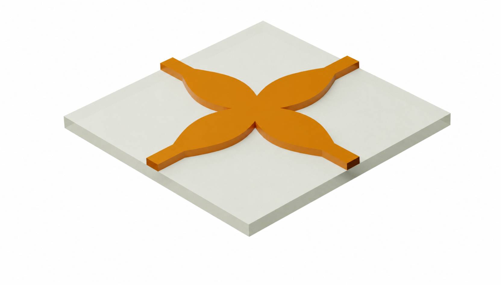
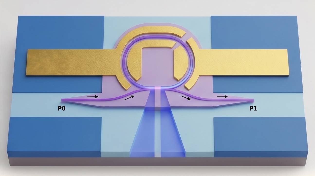
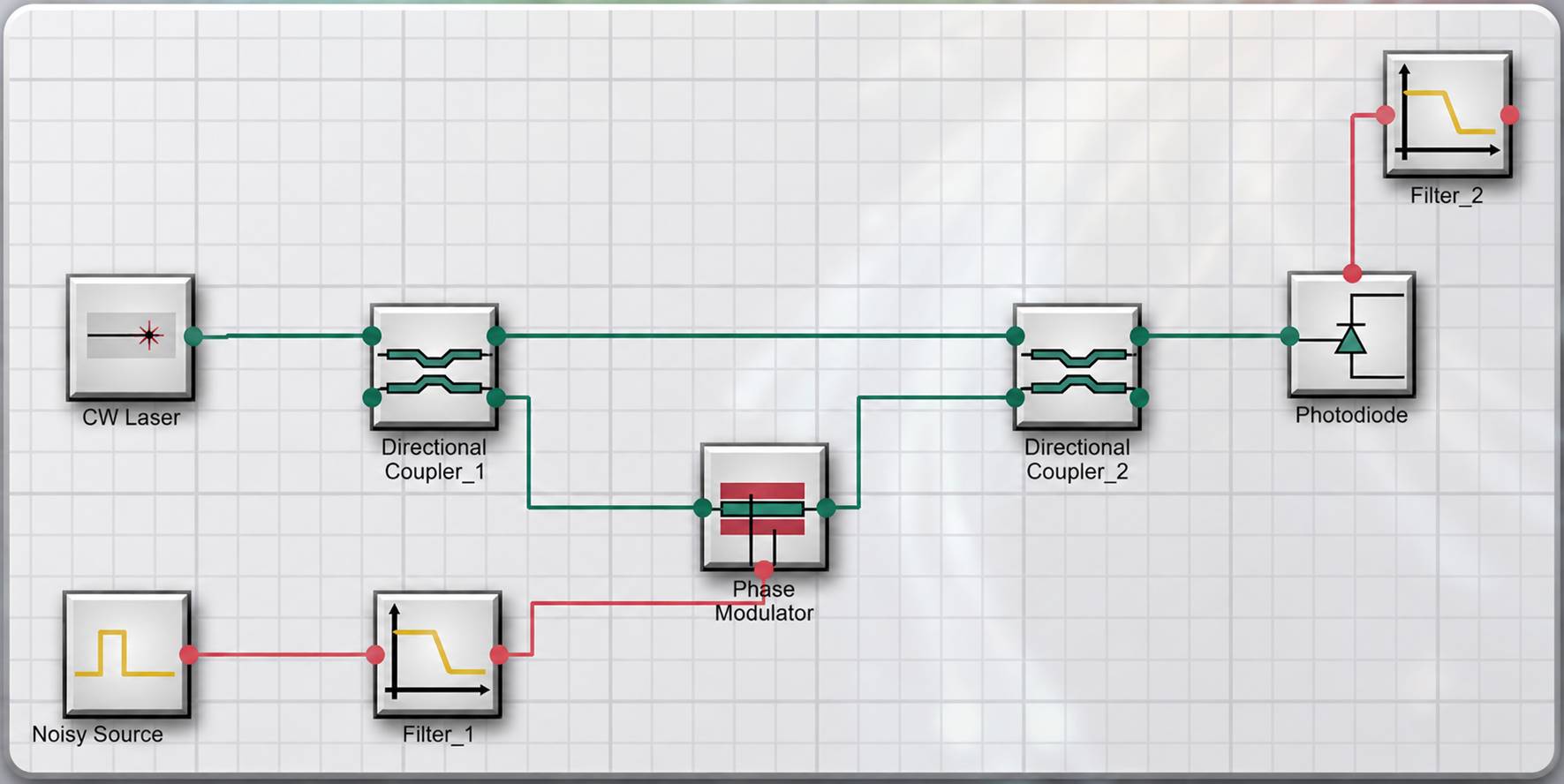
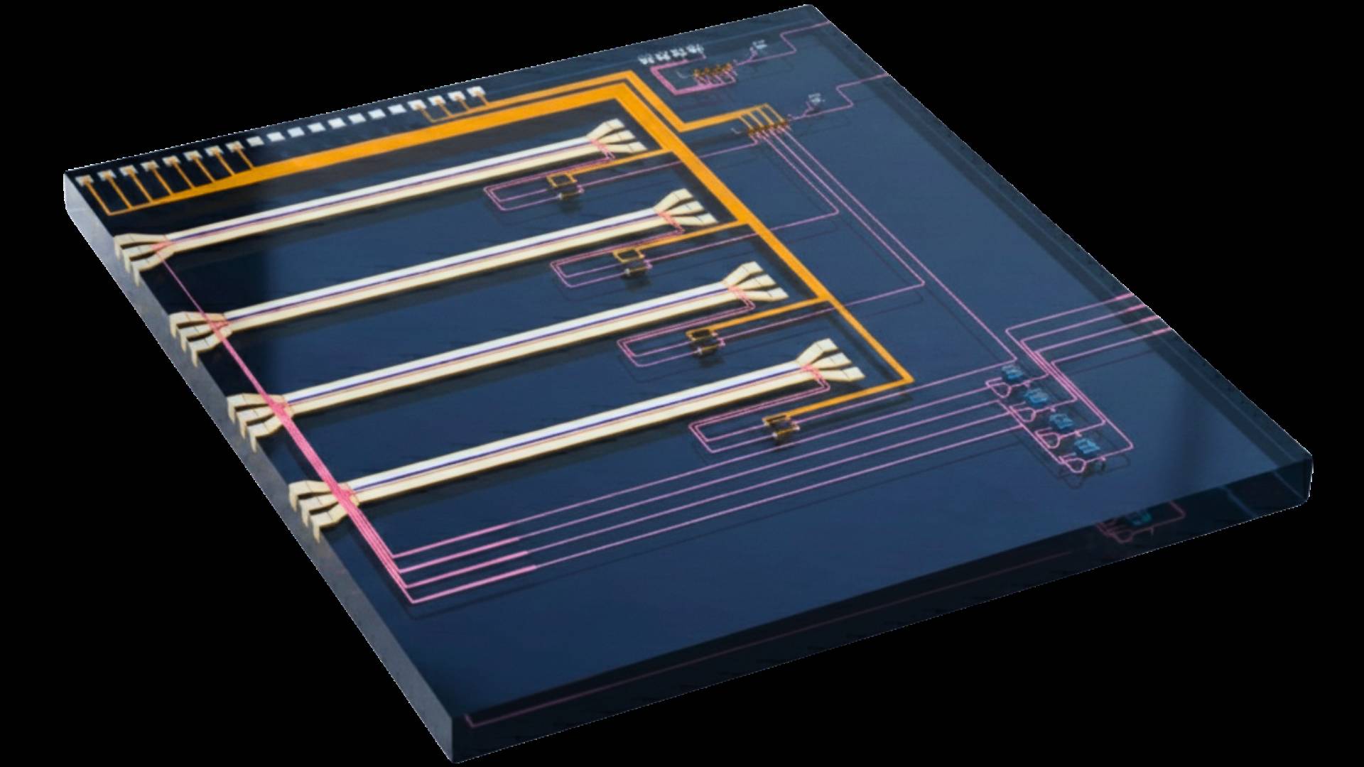
From a single primitive to a full chip - every level is a Component nesting the one before it.
Everything in PhotonForge is a Component - and that is true at every scale. A single waveguide is a Component, but so is a multi-element circuit and an entire chip. There is no separate "circuit" or "chip" type: larger systems are simply Components that nest smaller ones.
One Component can also hold several views of the same device. The layout view holds the physical shapes on each process layer. The schematic view holds the symbol and connectivity used to capture a circuit. Both describe the same object, so a change of intent is a change to one Component, not to two files that have to be kept in sync, and the ports and models described below travel with it.
Components contain all the geometrical and logical structures used to model and simulate the physical device. Most fabrication processes describe devices with a 2D layout (GDSII or OASIS), and PhotonForge components are defined by the same 2D geometries to integrate transparently with layout files. Components are composed hierarchically through Reference instances, so a coupler can sit inside an MZI, inside a transceiver circuit, inside a full reticle - each level reusing the level below: note how two references can point to the same component.
Technology and PDK
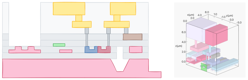
Simulating a device in 3D takes more information than a 2D layout carries: how thick each layer is, what material it is made of, how it is etched. That information comes from the intended fabrication process. Two terms for it are easy to mix up, so it is worth separating them clearly:
Because PhotonForge is released as a Python module, a PDK is simply another Python package that you install alongside it. Public PDKs install with pip, for example pip install siepic-forge, and expose their technology and component library as importable objects. Proprietary foundry PDKs are distributed by the foundry with their own installation instructions. You can also write a Technology yourself, layer by layer, when you are developing a process rather than consuming one.
Ports
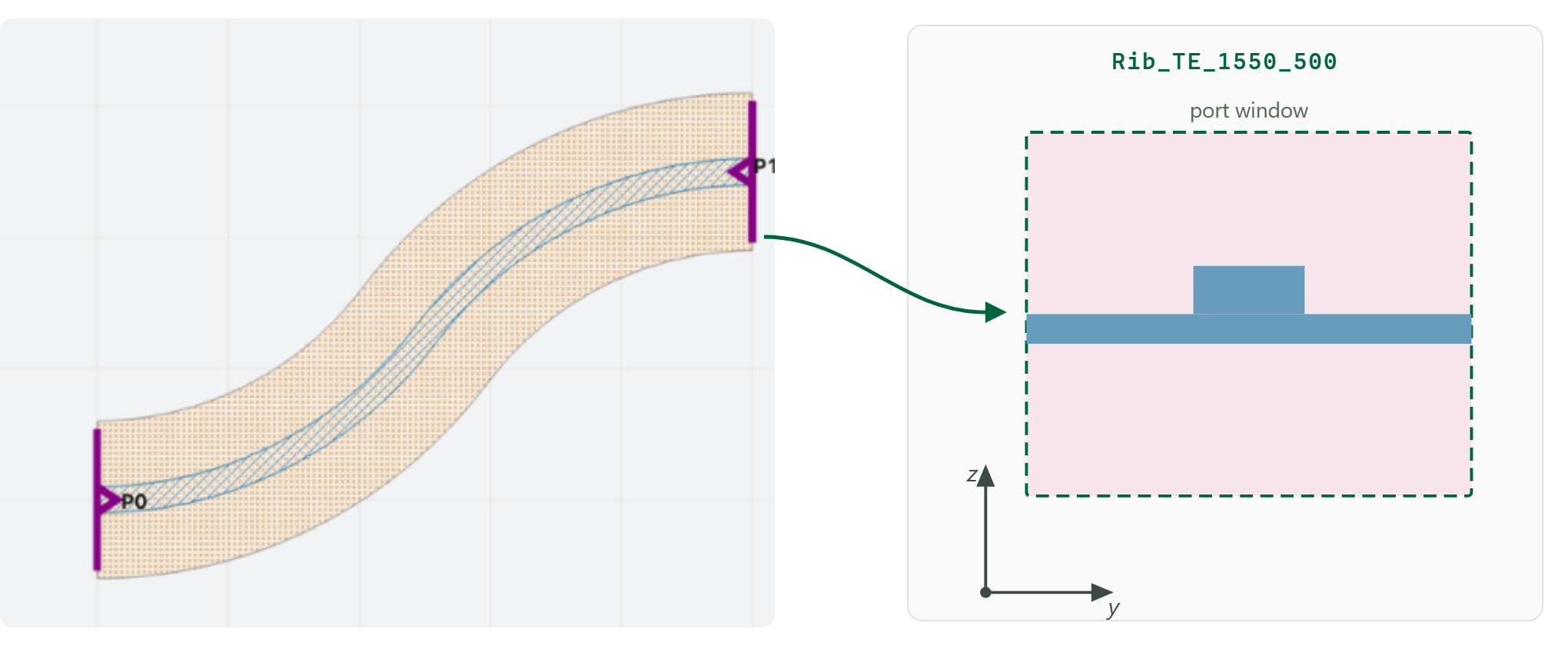
A Port marks the terminating cross-section of a waveguide, and it does two jobs at once:
A PhotonForge port carries more than a pin or a layout marker does. It knows its cross-section and the modes that cross-section supports, which is what lets the software excite the right mode and check that two connected ports are actually compatible. Ports also come in several kinds: optical waveguide ports, electrical ports and terminals, fiber ports for off-chip coupling, Gaussian ports for free-space beams, and virtual ports for models that carry a signal without any geometry to draw.
Models
To bridge the layout description of the device to its S parameters, a model is added to the component to perform that computation from the component's internal structures and ports. Models span a spectrum from instant-and-ideal to full-wave-and-exact, and the same component can carry different models as your design matures - prototype with an analytic model, then validate the critical block in FDTD without touching the layout.
The models are not a black box. The analytic building blocks ship as readable Python inside the package: photonforge.abstract is source you can open, read, and copy from, and the compact model guides walk through the equations one model at a time. So when a built-in model does not describe your device, you are not stuck: start from the closest analytic model, change what your physics requires, and attach the result to any component as a custom model.
Circuit & System Simulation
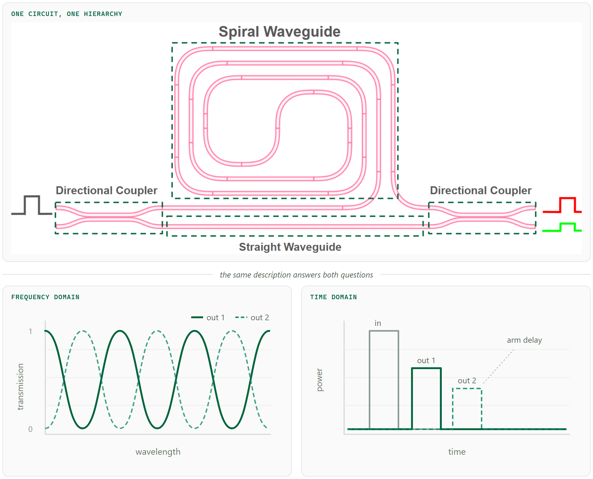
An unbalanced MZI, and the two regimes its single description feeds. Each dashed box is a sub-component with a model of its own.
Because a circuit (and a whole chip) is itself a Component, once its sub-components have models you can simulate the complete system - in two complementary regimes:
This simulation is layout-aware. You do not hand-build a netlist to go with your layout: PhotonForge walks down the component hierarchy, collects the model attached to each sub-component, and reads the connectivity from how the ports actually meet in the layout. Move a component, reroute a waveguide, or swap an analytic model for an FDTD result, and the next circuit simulation reflects it. The physical design and the system-level prediction cannot drift apart, because there is only one description of the circuit.
CircuitModel assembles sub-component S-matrices into the full circuit response - spectra, transmission, crosstalk, group delay.
Additional Capabilities
The Quick Start covers the core flow end to end. PhotonForge also covers the rest of the design and sign-off cycle:
RF & multiphysics
Lumped and distributed electrical models (RLC, transmission lines, CPW) for modulators, heaters and high-speed links.
Automatic routing
Waveguide and electrical connections generated port to port, around obstacles - single routes or whole bundles.
Design-rule checking (DRC)
Verify a layout against the foundry's manufacturing rules before tape-out.
Layout vs. schematic (LVS)
Confirm the physical layout matches the intended circuit netlist.
Inverse design & optimization
Gradient-based (autograd) shape optimization through FDTD, plus parameter sweeps with the design plugin.
Monte Carlo & yield
Propagate fabrication variability through the circuit to estimate performance spread and yield.
Nonlinear simulation
Time-domain circuit models capture nonlinear dynamics such as gain saturation and self-pulsing resonators.
Live Viewer
Inspect layouts interactively right in the notebook - zoom chip-scale designs, toggle layers, and cut cross-sections - no external layout viewer needed.
PDA SDK
The photonforge.pda Photonic Design Automation interface for managing versioned projects, libraries and automated flows.
GDSII / OASIS support
Import and export industry-standard layout formats (GDS-II and OASIS) for integration with any EDA tool or foundry PDK.


 TERMS & CONDITIONS

 How the process works:
 Try this real URL to see an example: