






Quick Start I
 Download this page as a notebook
Quick_Start.ipynb
Download this page as a notebook
Quick_Start.ipynb
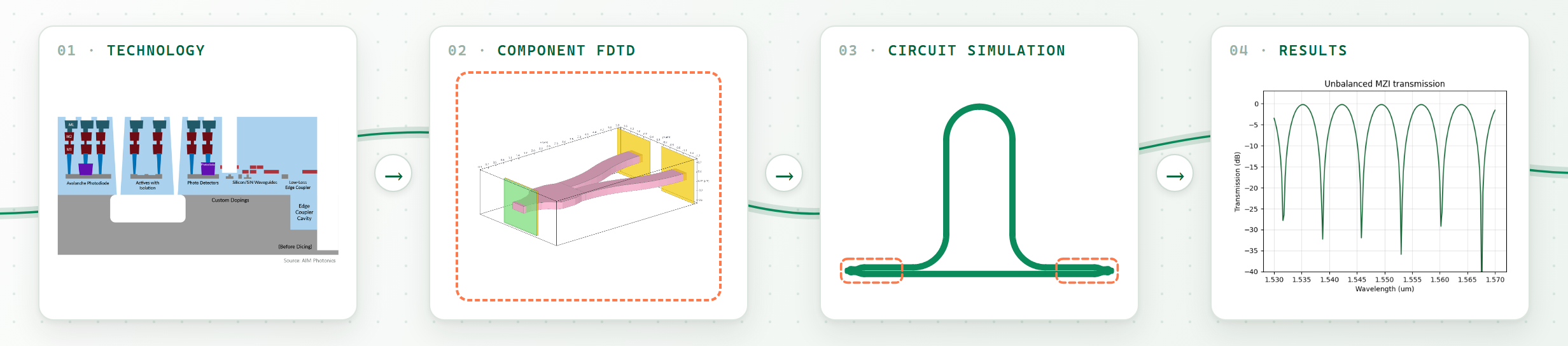
This quick start takes you from a foundry PDK to a simulated photonic circuit in five steps: load a PDK, import a component from a GDS file, verify it with 3D FDTD, assemble a Mach-Zehnder interferometer with PhotonForge's routing utilities, and simulate the full circuit. You only need PhotonForge and the open-source SiEPIC EBeam PDK:
pip install photonforge siepic-forgeStep 1: Loading a Foundry PDK
Foundry PDKs are loaded as PhotonForge technologies. A technology bundles everything the foundry process defines: layers, the extrusion recipe used to build 3D simulations, and the standard waveguide cross-sections (port specifications). Here we load the SiEPIC EBeam technology and set it as the default:
import numpy as np
  import photonforge as pf
  import siepic_forge as siepic_pdk
  from matplotlib import pyplot as plt

  technology = siepic_pdk.ebeam()
  pf.config.default_technology = technology
  technology
The technology also carries fabrication statistics from the foundry, which enable Monte Carlo yield analysis:
technology.random_variables[RandomVariable('si_thickness', **{'value': 0.22, 'stdev': 0.0037166666666666667})]We can plot the technology's layer stack in cross-section to see exactly what the foundry process looks like - the silicon device layer over the buried oxide, the heater metal, and the routing metal levels:
siepic_pdk.plot_cross_section(technology)
  plt.show()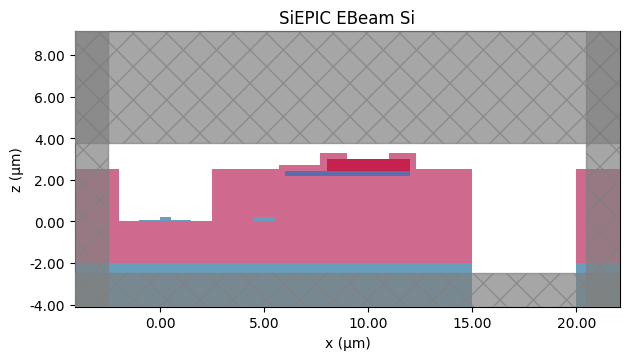
Cross-section of the SiEPIC EBeam layer stack.
Step 2: Loading a GDS Layout
Components can come from the PDK library, from parametric generators, or from any GDS file. Here we import a compact Y splitter layout (y_splitter.gds). This device was designed and optimized in the Y Splitter example - here we simply use the resulting GDS file, exactly as you would use a layout received from a colleague or another tool:
y_splitter = pf.load_layout("y_splitter.gds")["y_splitter"]
  y_splitter
The imported layout: geometry only, no ports and no models.
The imported component contains only geometry. Two ingredients make a layout simulation-ready: ports define where light enters and exits and which waveguide mode is used there, and a model defines how the component is simulated. PhotonForge can detect ports automatically from the geometry: we search the component boundaries for cross-sections that match the strip waveguide specification. (Ports can also be placed manually with Port when more control is needed.)
y_splitter.add_port(y_splitter.detect_ports(["TE_1550_500"], on_boundary="x"))
  y_splitter
The component with its input and output ports attached.
Finally we attach a Tidy3DModel,
which tells PhotonForge to compute this component's S parameters with a full 3D FDTD simulation in the cloud.
Attaching a model takes no configuration: the defaults come from the component and its technology.
y_splitter.add_model(pf.Tidy3DModel())
  y_splitter.active_model
Step 3: Convert 2D Layouts to 3D for Electromagnetic Simulation
PhotonForge automatically extrudes the 2D layout into a full 3D structure using the technology's extrusion specification - no manual 3D modeling required. We can inspect exactly what the FDTD solver will see - here, a top view of the extruded permittivity at the waveguide core:
pf.tidy3d_plot(y_splitter, z=0.11)
  plt.show()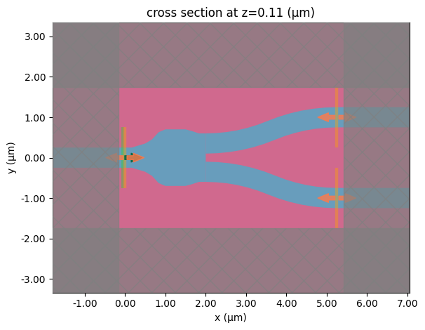
Top view of the extruded permittivity at the waveguide core.
Now we compute the S parameters. The simulation runs in the cloud and the result is cached, so re-running this cell (or reusing this component inside a larger circuit) does not re-simulate:
wavelengths = np.linspace(1.53, 1.57, 201)
  freqs = pf.C_0 / wavelengths

s_matrix = y_splitter.s_matrix(freqs)Starting...
Progress: 100%pf.plot_s_matrix(s_matrix, y="dB", input_ports=["P0"])
plt.show()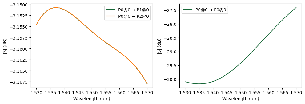
Transmission near the ideal -3 dB per arm, with reflection below -26 dB.
Step 4: Building an MZI with Routing
With a verified splitter in hand, we build an unbalanced Mach-Zehnder interferometer: the same Y
splitter is used twice (as splitter and combiner), and the two arms are created with the
route function. PhotonForge also
offers fully automatic, obstacle-aware routing with crossing insertion through
route_auto - for this simple
layout, plain point-to-point routing is all we need. The short arm is a direct route. For the long arm we pass
waypoints that create a U-shaped detour, and we choose the detour height to hit an exact path-length imbalance:
a U detour with a half-circle top adds 2h + 2r(π - 3) to the direct length, where h is the detour height and
r the bend radius:
mzi = pf.Component("mzi")

  splitter = mzi.add_reference(y_splitter)
  combiner = mzi.add_reference(y_splitter)
  combiner.rotate(180)
  combiner.translate((80, 0))

  radius = 10  # bend radius used by both arms (um)
  target_delta_l = 80.0  # extra path length wanted in the long arm (um)

  # Short arm: direct route
  arm_short = pf.parametric.route(
      port1=(splitter, "P1"), port2=(combiner, "P2"), radius=radius
  )

  # Long arm: U-shaped detour, its height set for an exact length imbalance
  height = target_delta_l / 2 - radius * (np.pi - 3)
  arm_long = pf.parametric.route(
      port1=(splitter, "P2"), port2=(combiner, "P1"), radius=radius,
      waypoints=[(40 - radius, 1 + height), (40 + radius, 1 + height)],
  )

  mzi.add_reference(arm_short)
  mzi.add_reference(arm_long)
  mzi
The routed MZI: straight lower arm, U-shaped detour in the upper arm.
The exact routed lengths are available through
route_length, which gives us the
physical path imbalance, and routing_collisions
verifies that no routes overlap:
length_short = pf.route_length(arm_short)
  length_long = pf.route_length(arm_long)
  delta_l = length_long - length_short

  print(f"Short arm: {length_short:.2f} um")
  print(f"Long arm:  {length_long:.2f} um")
print(f"Path imbalance: {delta_l:.2f} um")Short arm: 69.50 um
Long arm: 149.50 um
Path imbalance: 80.00 umStep 5: Circuit Simulation
To simulate the MZI we expose its input and output ports and attach a
CircuitModel.
A circuit model does not simulate any physics of its own. When you ask this MZI for its S matrix, the circuit model walks down the component hierarchy and finds every sub-component (here two Y splitter references and two routed arms), asks each one for its own S matrix, which invokes whatever model that sub-component carries, reads the connectivity from the layout - that is, from which ports actually meet - and cascades those S matrices into a single response for the whole circuit.
Two consequences are worth noticing. First, models mix freely: the Y splitter answers from its cached FDTD result, one cloud simulation reused for both references, while the routed arms answer from fast analytic waveguide models. Second, there is no netlist to maintain: the connectivity comes from the layout, so moving a component or rerouting an arm changes the next circuit simulation automatically, and the layout and the system-level prediction cannot drift apart.
mzi.add_port([splitter["P0"], combiner["P0"]])
  mzi.add_model(pf.CircuitModel())

mzi_s = mzi.s_matrix(freqs)transmission = np.abs(mzi_s[("P0@0", "P1@0")]) ** 2
plt.figure()
plt.plot(wavelengths, 10 * np.log10(transmission))
plt.xlabel("Wavelength (um)")
plt.ylabel("Transmission (dB)")
plt.title("Unbalanced MZI transmission")
plt.ylim(-40, 3)
plt.grid(True, alpha=0.3)
plt.show()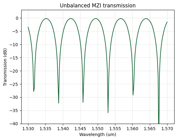
Interference fringes of the unbalanced MZI.
The interference fringes are exactly what the path imbalance predicts. The free spectral range of an unbalanced MZI is
where ng is the group index of the strip waveguide. The mode solver returns it
directly when asked with group_index=True, so we can compare:
modes = pf.port_modes("TE_1550_500", [pf.C_0 / 1.55], group_index=True)
  n_group = modes.data.n_group.item()

  fsr_theory = 1.55**2 / (n_group * delta_l) * 1000  # nm

  # Measured FSR from the spacing of transmission minima
  minima = [
      i for i in range(1, len(transmission) - 1)
      if transmission[i] < transmission[i - 1] and transmission[i] < transmission[i + 1]
  ]
  fsr_measured = np.diff(wavelengths[minima]).mean() * 1000  # nm

  print(f"Group index n_g = {n_group:.3f}")
  print(f"FSR (theory):    {fsr_theory:.2f} nm")
print(f"FSR (simulated): {fsr_measured:.2f} nm")Progress: 100%
Group index n_g = 4.181
FSR (theory): 7.18 nm
FSR (simulated): 7.20 nmNote: Theory and simulation agree to well under 1%.


 TERMS & CONDITIONS


 How the process works:
 Try this real URL to see an example: