





Author: Seokwoo Kim, POSTECH
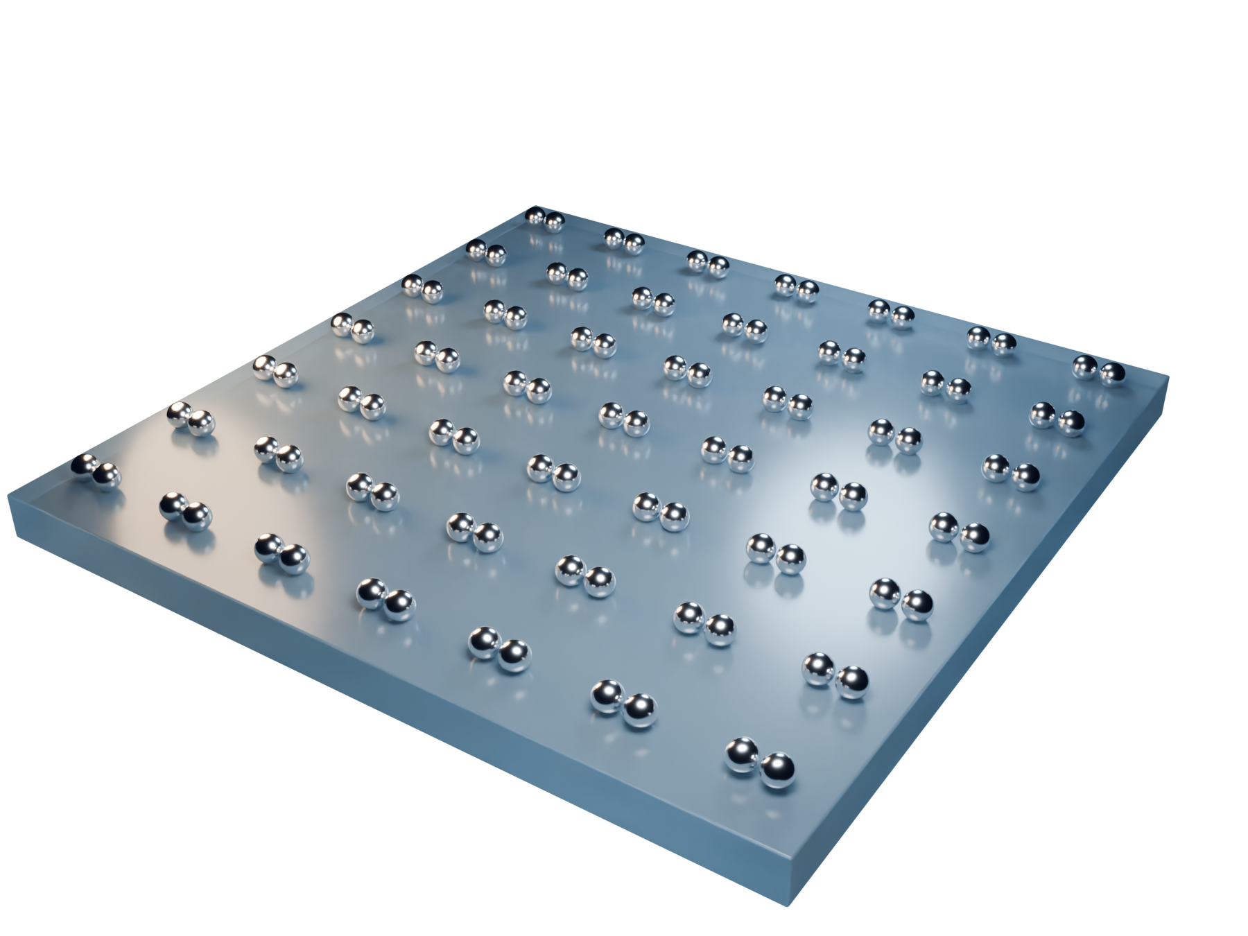
Two metal nanoparticles separated by a nanometre-scale gap support a bonding (gap) plasmon: the charges on the facing surfaces attract each other, the resonance red-shifts as the gap closes, and the electric field in the gap is strongly enhanced. These structures are popular for sensing, surface-enhanced spectroscopy and nonlinear optics, and they are a classic stress test for FDTD: the gap is one to two orders of magnitude smaller than the wavelength, and the metal surface is curved, so on a Cartesian grid it is represented by a staircase.
In this example we simulate a periodic array of silver nanosphere dimers (diameter 50 nm, gap 5 nm) under normal incidence and compare two local mesh sizes in the gap, 1 nm and 0.5 nm. We look at two different outputs of the same simulation:
- the far-field transmission and reflection spectrum, and
- the near-field intensity enhancement in the gap.
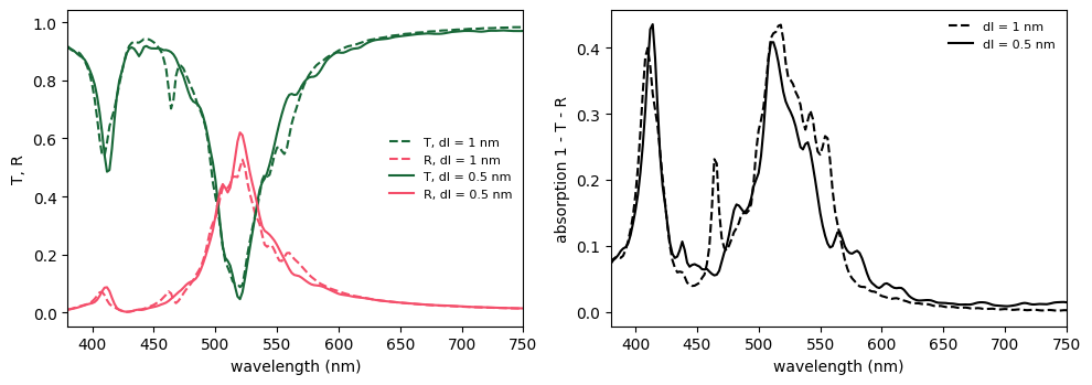
The point of the example is that these two outputs do not converge at the same rate. A mesh that is good enough for the spectrum is not necessarily good enough for the field enhancement, so the mesh should be chosen for the quantity you want to report.
import os

import matplotlib.pyplot as plt
import numpy as np
import tidy3d as td
from scipy.optimize import curve_fit
from tidy3d import web
Simulation Setup
Geometry. Two Ag spheres (diameter $D$ = 50 nm) are separated by a gap $g$ = 5 nm along $x$. The dimers form a square array with period 220 nm, which places the first diffraction order at $n \times 220 = 330$ nm, outside our 380–900 nm band. The particles sit on a glass substrate and are covered by an index-matching liquid, so the surrounding medium is homogeneous with $n$ = 1.5. This keeps the example free of a sphere–substrate contact point, which would be a second small feature competing with the gap.
Material. We use the Johnson–Christy silver model from the Tidy3D material library,
td.material_library["Ag"]["JohnsonChristy1972"].
Source. A plane wave at normal incidence, polarized along the dimer axis ($E \parallel x$), which excites the bonding mode.
nm = 1e-3  # Tidy3D length unit is um

# geometry (lengths written in nm, converted with "* nm")
D_nm, gap_nm = 50.0, 5  # sphere diameter, surface-to-surface gap
D, gap = D_nm * nm, gap_nm * nm
R = D / 2
period = 220.0 * nm  # array period in x and y
n_bg = 1.5  # index-matched glass environment
Lz = 1.2  # simulation size along z (um)

# materials
Ag = td.material_library["Ag"]["JohnsonChristy1972"]
background = td.Medium(permittivity=n_bg**2)

# wavelength / frequency range
lam = np.linspace(380, 900, 261) * nm
freqs = td.C_0 / lam
freq0 = 0.5 * (freqs.max() + freqs.min())
fwidth = freqs.max() - freqs.min()

for wl in (480, 520, 600):
    print(
        f"Ag permittivity at {wl} nm: {complex(Ag.eps_model(td.C_0 / (wl * nm))):.2f}"
    )
Ag permittivity at 480 nm: -8.54+0.16j
Ag permittivity at 520 nm: -10.83+0.20j
Ag permittivity at 600 nm: -15.81+0.32j
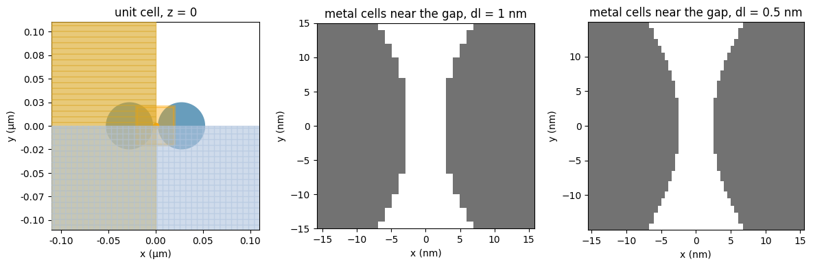
Mesh. The background mesh is automatic (20 steps per wavelength in the medium). On top of it we place two
MeshOverrideStructure boxes: one covering both particles with 1 nm steps, and a smaller box around the gap
(24 nm wide laterally) with the step dl_gap. With dl_gap = 1 nm the gap box is not needed.
Symmetry. For $E \parallel x$ the fields are antisymmetric (PEC-like) about the $x = 0$ plane and symmetric
(PMC-like) about $y = 0$, so symmetry=(-1, 1, 0) cuts the computational cost by four.
Subpixel treatment. Tidy3D's default for metals is Staircasing; we keep the default here so that the
mesh size is the only thing we change.
Monitors. Two flux monitors give $T$ and $R$. A point field monitor sits at the centre of the gap, and a small planar field monitor ($z = 0$, 40 nm × 40 nm) records the field map around the gap.
def make_sim(dl_gap, dl_body=1 * nm, run_time=300e-15):
    # two Ag spheres along x, gap centred at the origin
    xc = (D_nm / 2 + gap_nm / 2) * nm
    spheres = [
        td.Structure(
            geometry=td.Sphere(center=(s * xc, 0, 0), radius=D_nm / 2 * nm), medium=Ag
        )
        for s in (-1, 1)
    ]

    # local mesh refinement: whole dimer at dl_body, gap region at dl_gap
    overrides = [
        td.MeshOverrideStructure(
            geometry=td.Box(
                center=(0, 0, 0),
                size=((2 * D_nm + gap_nm + 4) * nm, (D_nm + 4) * nm, (D_nm + 4) * nm),
            ),
            dl=(dl_body,) * 3,
        )
    ]
    if dl_gap < dl_body:
        overrides.append(
            td.MeshOverrideStructure(
                geometry=td.Box(
                    center=(0, 0, 0), size=((gap_nm + 6) * nm, 24 * nm, 24 * nm)
                ),
                dl=(dl_gap,) * 3,
            )
        )
    grid_spec = td.GridSpec.auto(
        min_steps_per_wvl=20, wavelength=lam.min(), override_structures=overrides
    )

    source = td.PlaneWave(
        center=(0, 0, -0.45 * Lz),
        size=(td.inf, td.inf, 0),
        direction="+",
        pol_angle=0,  # E along x
        source_time=td.GaussianPulse(freq0=freq0, fwidth=fwidth),
    )
    monitors = [
        td.FluxMonitor(
            center=(0, 0, 0.42 * Lz), size=(td.inf, td.inf, 0), freqs=freqs, name="T"
        ),
        td.FluxMonitor(
            center=(0, 0, -0.48 * Lz), size=(td.inf, td.inf, 0), freqs=freqs, name="R"
        ),
        td.FieldMonitor(
            center=(0, 0, 0), size=(0, 0, 0), freqs=freqs, name="gap_center"
        ),
        td.FieldMonitor(
            center=(0, 0, 0),
            size=(40 * nm, 40 * nm, 0),
            freqs=freqs[::4],
            name="gap_plane",
        ),
    ]
    return td.Simulation(
        size=(period, period, Lz),
        medium=background,
        structures=spheres,
        sources=[source],
        monitors=monitors,
        grid_spec=grid_spec,
        run_time=run_time,
        shutoff=1e-5,
        boundary_spec=td.BoundarySpec(
            x=td.Boundary.periodic(), y=td.Boundary.periodic(), z=td.Boundary.pml()
        ),
        symmetry=(-1, 1, 0),
        subpixel=td.SubpixelSpec(
            metal=td.Staircasing()
        ),  # the default, written out explicitly
    )


sims = {"dl = 1 nm": make_sim(dl_gap=1 * nm), "dl = 0.5 nm": make_sim(dl_gap=0.5 * nm)}
Let us look at the structure and at the grid around the gap. The right-hand panels show the permittivity as it is assigned on the grid cells: the spheres become staircases, and with 1 nm cells the surface-to-surface distance on the dimer axis is quantised by the grid.
fig, axes = plt.subplots(1, 3, figsize=(12, 3.8))
sim = sims["dl = 0.5 nm"]
sim.plot(z=0, ax=axes[0])
axes[0].set_title("unit cell, z = 0")

zoom = td.Box(center=(0, 0, 0), size=(30 * nm, 30 * nm, 0))
for ax, (name, s) in zip(axes[1:], sims.items()):
    eps = s.epsilon(box=zoom, coord_key="centers", freq=td.C_0 / (520 * nm))
    ex = eps.real.squeeze()
    ax.pcolormesh(
        ex.x / nm,
        ex.y / nm,
        (ex < 0).T,
        cmap="Greys",
        shading="nearest",
        vmin=0,
        vmax=1.6,
    )
    ax.set_aspect("equal")
    ax.set_xlabel("x (nm)")
    ax.set_ylabel("y (nm)")
    ax.set_title(f"metal cells near the gap, {name}")
plt.tight_layout()
plt.show()
Running the Simulations
Always check the cost before running. web.estimate_cost returns an upper bound; because the field decays below
the shutoff level before run_time is reached, the billed cost is usually lower. In our runs the estimates were
0.039 FlexCredit (1 nm) and 0.137 FlexCredit (0.5 nm), and the billed costs were 0.025 and 0.077 FlexCredit.
The helper below reuses saved results when they exist, so the notebook can be re-executed without
running the simulations again. Set CHECK_COST = True to print the estimates first.
CHECK_COST = False
os.makedirs("data", exist_ok=True)
files = {
    "dl = 1 nm": "data/g5_dl1_stair.hdf5",
    "dl = 0.5 nm": "data/g5_dl0.5_stair.hdf5",
}

if CHECK_COST:
    for name, s in sims.items():
        task_id = web.upload(s, task_name=f"ag_dimer_{name}")
        print(name, web.estimate_cost(task_id))

data = {}
for name, s in sims.items():
    if os.path.exists(files[name]):
        data[name] = td.SimulationData.from_file(files[name])
        # make sure the stored result belongs to exactly this simulation
        assert data[name].simulation == s, (
            "saved data does not match the current simulation"
        )
    else:
        data[name] = web.run(s, task_name=f"ag_dimer_{name}", path=files[name])
print("loaded:", list(data))
loaded: ['dl = 1 nm', 'dl = 0.5 nm']
def spectra(sim_data):
    f = sim_data["T"].flux.f.values
    order = np.argsort(td.C_0 / f)
    wl = (td.C_0 / f)[order] / nm
    T = sim_data["T"].flux.values[order]
    R = -sim_data["R"].flux.values[order]
    return wl, T, R


def lorentz_dip(x, a, x0, w, c, s):
    return c + s * (x - x0) - a * w**2 / ((x - x0) ** 2 + w**2)


def fit_dip(wl, T, lo=470, hi=650):
    sel = (wl > lo) & (wl < hi)
    x0 = wl[sel][np.argmin(T[sel])]
    win = (wl > x0 - 30) & (wl < x0 + 30)
    p, _ = curve_fit(lorentz_dip, wl[win], T[win], p0=[0.8, x0, 20, 0.9, 0])
    return p[1], 2 * abs(p[2])


fig, ax = plt.subplots(1, 2, figsize=(10, 3.6))
res = {}
for (name, d), ls in zip(data.items(), ["--", "-"]):
    wl, trans, refl = spectra(d)
    res[name] = fit_dip(wl, trans)
    ax[0].plot(wl, trans, ls, color="C0", label=f"T, {name}")
    ax[0].plot(wl, refl, ls, color="C3", label=f"R, {name}")
    ax[1].plot(wl, 1 - trans - refl, ls, color="k", label=name)
ax[0].set_ylabel("T, R")
ax[1].set_ylabel("absorption 1 - T - R")
for a in ax:
    a.set_xlabel("wavelength (nm)")
    a.set_xlim(380, 750)
    a.legend(frameon=False, fontsize=8)
plt.tight_layout()
plt.show()

for name, (x0, fw) in res.items():
    print(f"{name:12s}: bonding-mode dip at {x0:6.1f} nm, FWHM {fw:4.1f} nm")
dl = 1 nm   : bonding-mode dip at  514.7 nm, FWHM 48.1 nm
dl = 0.5 nm : bonding-mode dip at  516.5 nm, FWHM 44.5 nm
The main transmission dip near 515 nm is the bonding mode of the dimer array (the shorter-wavelength dip near 410 nm is not analysed here). Halving the gap mesh moves it by about 2 nm, which is small compared with its ~45 nm width. The 1 nm spectrum also shows a narrow extra feature near 465 nm that is absent at 0.5 nm, so we attribute it to the coarse staircase rather than to a physical mode. A narrow feature should survive a mesh refinement before it is interpreted.
Near Field: Enhancement in the Gap
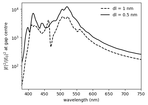
The plane wave is normalised to unit power through the unit cell, so the incident intensity in the medium is $|E_0|^2 = 2 Z_0 / (n A)$, where $A$ is the unit-cell area and $Z_0$ the vacuum impedance. (A run of the same cell without particles reproduced this value within 1 %.) We plot the enhancement $|E|^2/|E_0|^2$ at the centre of the gap.
E0_sq = 2 * td.ETA_0 / (n_bg * period**2)


def intensity(field_data):
    return sum(np.abs(field_data.field_components[c]) ** 2 for c in ("Ex", "Ey", "Ez"))


fig, ax = plt.subplots(figsize=(5, 3.6))
enh = {}
for (name, d), ls in zip(data.items(), ["--", "-"]):
    I = intensity(d["gap_center"]).squeeze()
    wl_c = td.C_0 / I.f.values / nm
    o = np.argsort(wl_c)
    ax.semilogy(wl_c[o], I.values[o] / E0_sq, ls, color="k", label=name)
    enh[name] = np.interp(res[name][0], wl_c[o], I.values[o] / E0_sq)
ax.set_xlabel("wavelength (nm)")
ax.set_ylabel(r"$|E|^2/|E_0|^2$ at gap centre")
ax.set_xlim(380, 750)
ax.legend(frameon=False)
plt.tight_layout()
plt.show()

for name in data:
    print(
        f"{name:12s}: |E|^2/|E0|^2 at the gap centre, at the dip wavelength = {enh[name]:7.0f}"
    )
print(f"ratio 0.5 nm / 1 nm = {enh['dl = 0.5 nm'] / enh['dl = 1 nm']:.2f}")
dl = 1 nm   : |E|^2/|E0|^2 at the gap centre, at the dip wavelength =    4737
dl = 0.5 nm : |E|^2/|E0|^2 at the gap centre, at the dip wavelength =   11158
ratio 0.5 nm / 1 nm = 2.36
The spectrum barely moved, but the gap-centre enhancement changed by a factor of about 2.4. With 1 nm cells the 5 nm gap is resolved by only a handful of cells, and the staircase changes the local surface-to-surface distance, to which the gap field is far more sensitive than the far-field resonance is.
Field Map of the Gap Mode
Finally, we plot the field map in the $z = 0$ plane at the monitor frequency closest to the transmission dip (0.5 nm mesh). The field is concentrated in the gap and is largest next to the metal surface.
name = "dl = 0.5 nm"
I = intensity(data[name]["gap_plane"]).squeeze()
wl_p = td.C_0 / I.f.values / nm
k = np.argmin(np.abs(wl_p - res[name][0]))
Ik = I.isel(f=k)

fig, ax = plt.subplots(figsize=(4.6, 3.8))
im = ax.pcolormesh(
    Ik.x / nm,
    Ik.y / nm,
    np.log10(Ik.values.T / E0_sq),
    cmap="magma",
    shading="auto",
    vmin=0,
    vmax=5.5,
)
for s in (-1, 1):  # nominal sphere outlines
    ax.add_patch(
        plt.Circle(
            (s * (R + gap / 2) / nm, 0), R / nm, fill=False, color="w", lw=0.6, ls="--"
        )
    )
ax.set_aspect("equal")
ax.set_xlim(-20, 20)
ax.set_ylim(-20, 20)
ax.set_xlabel("x (nm)")
ax.set_ylabel("y (nm)")
ax.set_title(f"{wl_p[k]:.0f} nm, {name}")
plt.colorbar(im, ax=ax, label=r"$\log_{10}(|E|^2/|E_0|^2)$")
plt.tight_layout()
plt.show()
print(f"max |E|^2/|E0|^2 in this plane: {float(Ik.max()) / E0_sq:.3g}")
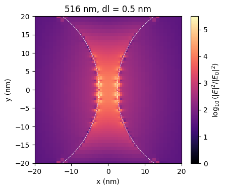
max |E|^2/|E0|^2 in this plane: 7.46e+04
The maximum of this map sits on the staircased metal surface, not in the middle of the gap. Its value depends on where the grid corners fall, so a maximum over the map is not a mesh-converged quantity; quote the field at the gap centre (or its mean over the gap volume) instead.
Takeaways
- For a 5 nm gap, the far-field bonding resonance moved by about 2 nm when the gap mesh was halved from 1 nm to 0.5 nm, while the gap-centre intensity enhancement changed by a factor of about 2.4. The spectrum converges at a coarser mesh than the near field.
- In a separate check (not included here, about 0.35 FlexCredit) we refined the gap mesh further to 0.25 nm: the resonance moved by less than 2 nm again and the gap-centre enhancement by about 6 %. For this geometry, about 10 cells across the gap (0.5 nm for a 5 nm gap) were needed for the near field, and about 5 cells (1 nm) for the spectrum.
- Peak values of $|E|^2$ on a staircased metal surface do not converge with mesh refinement and should not be reported as "the enhancement".
- There is no universal cells-per-gap rule. In a similar check with a 2 nm gap, the fitted resonance still moved from 584 nm to 575 nm between 0.5 nm and 0.25 nm cells, so 8 cells across the gap were not enough there. Always halve the mesh at least once, and judge convergence on the quantity you will report.
References
- A. Calà Lesina, A. Vaccari, P. Berini, L. Ramunno, "On the convergence and accuracy of the FDTD method for nanoplasmonics," Opt. Express 23, 10481 (2015). doi:10.1364/OE.23.010481
- I. Romero, J. Aizpurua, G. W. Bryant, F. J. García de Abajo, "Plasmons in nearly touching metallic nanoparticles: singular response in the limit of touching dimers," Opt. Express 14, 9988 (2006). doi:10.1364/OE.14.009988


 TERMS & CONDITIONS


 How the process works:
 Try this real URL to see an example: