





import pickle

import autograd.numpy as anp
import matplotlib.pyplot as plt
import numpy as np
from autograd.tracer import getval

import tidy3d as td
import tidy3d.web as web
from tidy3d.plugins.autograd import adam, apply_updates, rescale, value_and_grad
from tidy3d.plugins.autograd.invdes import (
    make_conic_filter,
    make_erosion_dilation_penalty,
    symmetrize_mirror,
    tanh_projection,
)
TIDY3D
LEARNING CENTER
Example Library

Inverse designed waveguide reflector and Fabry-Perot cavity
Note: the cost of running the entire notebook is larger than 10 FlexCredits.
Compact on-chip mirrors are a key building block for integrated Fabry-Perot cavities, laser feedback sections, and sensing. A broadband, high-reflectivity mirror is difficult to realize with conventional Bragg gratings in a small footprint, which makes it an excellent target for adjoint-based topology optimization.
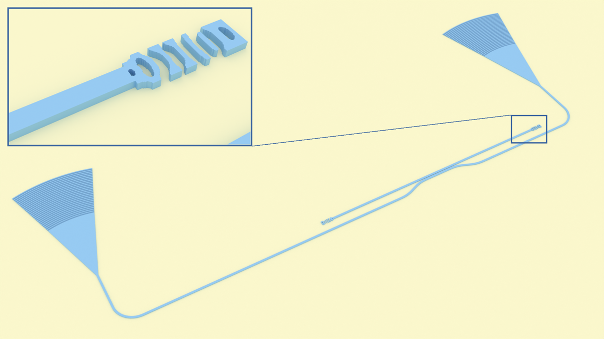
In this notebook, we demonstrate the complete design flow of a terminating waveguide reflector on the 220 nm silicon-on-insulator platform with oxide cladding: a \(1 \times 3\) \(\mu m\) design region attached to a 500 nm single-mode waveguide is optimized to reflect the fundamental TE mode back into the waveguide, reaching about 99% reflectivity at 1550 nm while respecting a 100 nm minimum feature size in a fully binarized layout. We then assemble two copies of the mirror into a side-coupled Fabry-Perot cavity and compute its circuit-level spectrum, which shows a free spectral range of about 4.7 nm, deep on-resonance extinction, and a loaded quality factor of several thousand. Finally, we attach grating couplers following the SiEPIC layout conventions to produce a fabrication-ready chip layout.
The workflow has six parts: 1 robust inverse design of the reflector, 2 binarization and minimum-feature-size enforcement, 3 high-accuracy verification and GDS export, 4 cavity circuit assembly and simulation with PhotonForge on the SiEPIC PDK, 5 quality factor extraction, and 6 the fabrication-ready layout with grating couplers.
For more inverse design examples, please visit our examples page. If you are new to the finite-difference time-domain (FDTD) method, we highly recommend going through our FDTD101 tutorials.
Inverse Design Setup
We define the wavelength, the constant-index silicon and oxide used during optimization, and the design-region geometry. The design region is discretized into 20 nm pixels. The conic filter radius of 150 nm deliberately exceeds the 100 nm fabrication limit: the margin keeps the thresholded design legal.
lda0 = 1.55                       # central wavelength (um)
freq0 = td.C_0 / lda0
fwidth = freq0 / 10
eps_si = 3.48**2                  # constant-index materials for optimization
eps_sio2 = 1.444**2

wg_width = 0.50                   # SiEPIC-native single-mode strip width (um)
t_slab = 0.22                     # silicon thickness (um)
lx_des, ly_des = 3.0, 1.0         # design region (um)
pix = 0.02                        # design pixel size (um)
nx, ny = int(lx_des / pix), int(ly_des / pix)
min_feature = 0.100               # required minimum feature size (um)
filter_radius = 0.150             # conic filter radius (um), margin above min_feature
etas = (0.45, 0.5, 0.55)          # dilated / nominal / eroded projections
beta_final = 50.0
num_steps = 35
penalty_weight = 2.0

Lx, Ly, Lz = 7.0, 3.4, 2.4        # simulation domain (um)
x_src = -lx_des / 2 - 0.7
x_refl = x_src - 0.5
mode_plane = (0, 2.2, 1.6)
mode_spec = td.ModeSpec(num_modes=1, target_neff=3.5)

conic_filter = make_conic_filter(filter_radius, pix)
penalty_fn = make_erosion_dilation_penalty(filter_radius, pix)
The reflector is a terminating mirror: the input waveguide extends through the boundary on one side and plain oxide lies beyond the design region on the other. We record the reflected fundamental mode with a ModeMonitor placed behind the ModeSource, so it only sees the backward-propagating wave. A MeshOverrideStructure locks the FDTD grid to the design pixels, and symmetry=(0,-1,1) exploits the two mirror symmetries of the TE mode for a fourfold cost reduction.
def make_sim_base(msw: int = 18, override_dl=(pix, pix, pix), freqs=(freq0,), with_field: bool = False) -> td.Simulation:
    """Terminating-mirror FDTD without the design region."""
    wg_in = td.Structure(
        geometry=td.Box.from_bounds(
            rmin=(-1e3, -wg_width / 2, -t_slab / 2), rmax=(-lx_des / 2, wg_width / 2, t_slab / 2)
        ),
        medium=td.Medium(permittivity=eps_si),
    )
    mode_source = td.ModeSource(
        source_time=td.GaussianPulse(freq0=freq0, fwidth=fwidth),
        center=(x_src, 0, 0),
        size=mode_plane,
        mode_index=0,
        mode_spec=mode_spec,
        direction="+",
    )
    monitors = [
        td.ModeMonitor(center=(x_refl, 0, 0), size=mode_plane, freqs=list(freqs), mode_spec=mode_spec, name="refl")
    ]
    if with_field:
        monitors.append(
            td.FieldMonitor(center=(0, 0, 0), size=(td.inf, td.inf, 0), freqs=[freq0], name="field")
        )
    mesh = td.MeshOverrideStructure(
        geometry=td.Box(center=(0, 0, 0), size=(lx_des, ly_des, t_slab)), dl=list(override_dl), enforce=True
    )
    return td.Simulation(
        size=(Lx, Ly, Lz),
        medium=td.Medium(permittivity=eps_sio2),
        grid_spec=td.GridSpec.auto(min_steps_per_wvl=msw, wavelength=lda0, override_structures=[mesh]),
        structures=[wg_in],
        sources=[mode_source],
        monitors=monitors,
        run_time=1.5e-12,
        boundary_spec=td.BoundarySpec.all_sides(boundary=td.PML()),
        symmetry=(0, -1, 1),
    )


def make_design_structure(eps_2d) -> td.Structure:
    """Bind a (traced) permittivity array to the design-region box as a custom medium."""
    box = td.Box(center=(0, 0, 0), size=(lx_des, ly_des, t_slab))
    return td.Structure.from_permittivity_array(geometry=box, eps_data=eps_2d.reshape((nx, ny, 1)))
Before submitting anything, we visualize the initial simulation with the uniform gray design to make sure all components are placed correctly.
params0 = 0.5 * np.ones((nx, ny))
d0 = tanh_projection(conic_filter(symmetrize_mirror(params0, axis=1)), 1.0, 0.5)
sim_preview = make_sim_base().updated_copy(
    structures=[*make_sim_base().structures, make_design_structure(rescale(d0, eps_sio2, eps_si))]
)

fig, (ax1, ax2) = plt.subplots(1, 2, figsize=(12, 4), tight_layout=True)
sim_preview.plot_eps(z=0, ax=ax1, freq=freq0)
sim_preview.plot_eps(x=0, ax=ax2, freq=freq0)
plt.show()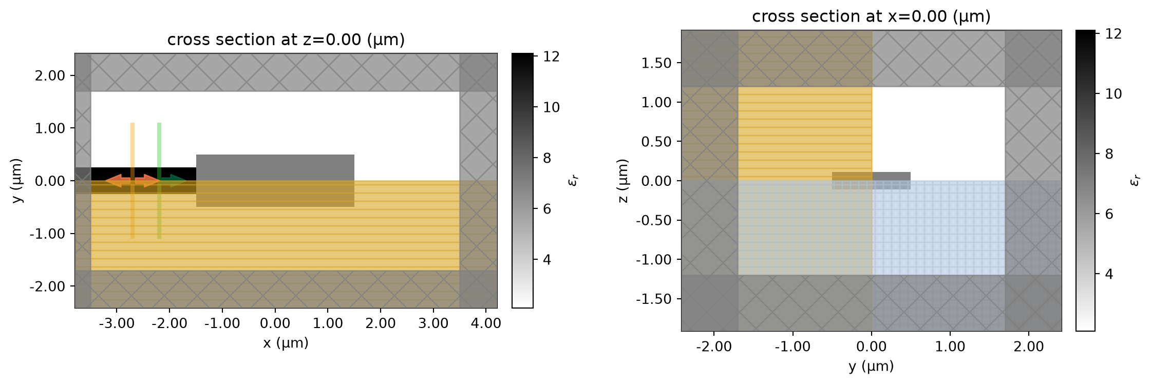
The objective is robust to fabrication bias and to the final thresholding step: each gradient evaluation simulates three versions of the design, projected at \(\eta = 0.45\), \(0.5\), and \(0.55\) (dilated, nominal, eroded), and averages their logarithmic reflection objectives. The average, rather than the worst case, keeps all three adjoint sources well conditioned. The erosion-dilation fabrication penalty is evaluated on the design padded with its physical surroundings (waveguide on the left, oxide on the right); without the padding the penalty cannot see sub-100 nm gaps pinched against the waveguide junction.
aux = {}  # per-step diagnostics recorded by the objective


def objective(params, beta: float, task_name: str) -> float:
    """Mean of log-reflection objectives over eroded/nominal/dilated projections, minus the fabrication penalty."""
    p = symmetrize_mirror(params, axis=1)
    filtered = conic_filter(p)
    sims, dens = {}, {}
    for tag, eta in zip(("dil", "nom", "ero"), etas):
        d = tanh_projection(filtered, beta, eta)
        dens[tag] = d
        base = make_sim_base()
        sims[tag] = base.updated_copy(
            structures=[*base.structures, make_design_structure(rescale(d, eps_sio2, eps_si))]
        )
    batch = web.run(sims, task_name=task_name, verbose=False)
    Rs = [
        anp.sum(anp.abs(batch[t]["refl"].amps.sel(direction="-", f=freq0, mode_index=0).values) ** 2)
        for t in ("dil", "nom", "ero")
    ]
    logs = [-anp.log10(1.0 - r + 1e-6) for r in Rs]
    wg_col = (np.abs((np.arange(ny) - (ny - 1) / 2) * pix) <= wg_width / 2).astype(float)
    padded = anp.concatenate([np.tile(wg_col, (8, 1)), dens["nom"], np.zeros((8, ny))], axis=0)
    pen = penalty_fn(padded)
    weight = min(1.0, beta / 25.0) * penalty_weight
    J = (logs[0] + logs[1] + logs[2]) / 3.0 - weight * pen
    aux.update(R=float(getval(Rs[1])), R_worst=float(min(getval(r) for r in Rs)), pen=float(getval(pen)))
    return J


val_grad = value_and_grad(objective)
Now we run the optimization with the Adam optimizer and a linear \(\beta\) ramp from 1 to 50, which gradually binarizes the design. The history is saved to disk after every iteration so a long run is never lost.
optimizer = adam(learning_rate=0.1)
params = params0.copy()
opt_state = optimizer.init(params)
history = {"J": [], "R": [], "R_worst": [], "pen": [], "params": []}

betas = np.linspace(1.0, beta_final, num_steps)
for i in range(num_steps):
    J, grad = val_grad(params, betas[i], task_name=f"reflector_step_{i:03d}")
    updates, opt_state = optimizer.update(-grad, opt_state, params)  # -grad: maximize J
    params[:] = apply_updates(params, updates)
    np.clip(params, 0.0, 1.0, out=params)
    history["J"].append(float(J))
    history["R"].append(aux["R"])
    history["R_worst"].append(aux["R_worst"])
    history["pen"].append(aux["pen"])
    history["params"].append(params.copy())
    with open("reflector_history.pkl", "wb") as f:
        pickle.dump(history, f)
    print(
        f"step {i+1:2d}/{num_steps}: J={J:+.4f} R_nom={100*aux['R']:.3f}% "
        f"R_worst={100*aux['R_worst']:.3f}% pen={aux['pen']:.3f}"
    )
step 1/35: J=-0.0432 R_nom=7.224% R_worst=4.974% pen=0.943
step 2/35: J=+0.1725 R_nom=64.957% R_worst=36.793% pen=0.944
step 3/35: J=+0.7432 R_nom=95.520% R_worst=78.261% pen=0.945
step 4/35: J=+0.9899 R_nom=96.747% R_worst=94.849% pen=0.940
step 5/35: J=+0.9679 R_nom=96.563% R_worst=96.033% pen=0.908
step 6/35: J=+0.9516 R_nom=97.107% R_worst=96.662% pen=0.868
step 7/35: J=+0.9415 R_nom=97.618% R_worst=96.473% pen=0.824
step 8/35: J=+0.9641 R_nom=97.846% R_worst=97.201% pen=0.772
step 9/35: J=+0.9654 R_nom=98.186% R_worst=97.481% pen=0.732
step 10/35: J=+0.8974 R_nom=98.251% R_worst=97.627% pen=0.692
step 11/35: J=+0.9393 R_nom=98.381% R_worst=97.923% pen=0.644
step 12/35: J=+0.9283 R_nom=98.550% R_worst=97.875% pen=0.609
step 13/35: J=+0.9045 R_nom=98.533% R_worst=98.034% pen=0.590
step 14/35: J=+0.9398 R_nom=98.785% R_worst=98.435% pen=0.574
step 15/35: J=+0.8925 R_nom=98.752% R_worst=98.292% pen=0.563
step 16/35: J=+0.8716 R_nom=98.819% R_worst=98.372% pen=0.555
step 17/35: J=+0.8456 R_nom=98.884% R_worst=98.437% pen=0.537
step 18/35: J=+0.8600 R_nom=98.965% R_worst=98.566% pen=0.519
step 19/35: J=+0.9052 R_nom=98.931% R_worst=98.647% pen=0.508
step 20/35: J=+0.9544 R_nom=99.104% R_worst=98.561% pen=0.498
step 21/35: J=+0.9854 R_nom=99.140% R_worst=98.630% pen=0.489
step 22/35: J=+1.0054 R_nom=99.101% R_worst=98.832% pen=0.484
step 23/35: J=+0.9949 R_nom=99.011% R_worst=98.805% pen=0.481
step 24/35: J=+1.0595 R_nom=99.169% R_worst=98.902% pen=0.478
step 25/35: J=+1.0470 R_nom=99.089% R_worst=98.888% pen=0.475
step 26/35: J=+1.0572 R_nom=99.151% R_worst=98.825% pen=0.474
step 27/35: J=+1.0694 R_nom=99.254% R_worst=98.890% pen=0.474
step 28/35: J=+1.0763 R_nom=99.193% R_worst=98.896% pen=0.473
step 29/35: J=+1.1068 R_nom=99.174% R_worst=99.022% pen=0.470
step 30/35: J=+1.1033 R_nom=99.163% R_worst=99.049% pen=0.470
step 31/35: J=+1.1164 R_nom=99.101% R_worst=99.026% pen=0.469
step 32/35: J=+1.0979 R_nom=99.122% R_worst=99.037% pen=0.467
step 33/35: J=+1.1095 R_nom=99.149% R_worst=98.986% pen=0.464
step 34/35: J=+1.1142 R_nom=99.162% R_worst=98.982% pen=0.460
step 35/35: J=+1.1239 R_nom=99.167% R_worst=98.995% pen=0.458We plot the optimization history: the nominal and worst-case reflectivities converge together, which is exactly the robustness the three-projection objective buys.
steps = np.arange(1, len(history["J"]) + 1)
fig, (ax1, ax2) = plt.subplots(1, 2, figsize=(12, 4), tight_layout=True)
ax1.plot(steps, history["J"], "-o", ms=3)
ax1.set_xlabel("Iteration")
ax1.set_ylabel("Objective")
ax1.grid()
ax2.plot(steps, 100 * np.array(history["R"]), "-o", ms=3, label="nominal")
ax2.plot(steps, 100 * np.array(history["R_worst"]), "-s", ms=3, label="worst projection")
ax2.set_xlabel("Iteration")
ax2.set_ylabel("Reflectivity (%)")
ax2.legend()
ax2.grid()
plt.show()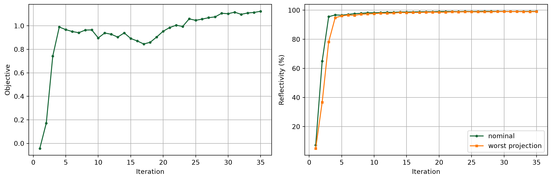
Binarization and Minimum Feature Size
The optimized gray-scale density must become a fully binary silicon/oxide layout that respects the 100 nm minimum feature size everywhere, including against the waveguide junction. We implement the morphological checks with plain numpy: disk-based opening flags undersized silicon features, disk-based closing flags undersized oxide gaps, and a flood fill groups violations into clusters. Clusters smaller than 6 pixels are convex corner tips, which lithography rounds anyway; larger clusters are genuine violations that we repair directionally, filling undersized gaps and dilating thin walls.
pad = 8
d100 = [(dx, dy) for dx in range(-3, 4) for dy in range(-3, 4) if dx**2 + dy**2 <= (min_feature / 2 / pix) ** 2 + 1e-9]
d3x3 = [(dx, dy) for dx in range(-1, 2) for dy in range(-1, 2)]


def shift(a, dx: int, dy: int):
    """Shift a 2D bool array, filling with False."""
    out = np.zeros_like(a)
    out[max(dx, 0) : a.shape[0] + min(dx, 0), max(dy, 0) : a.shape[1] + min(dy, 0)] = a[
        max(-dx, 0) : a.shape[0] + min(-dx, 0), max(-dy, 0) : a.shape[1] + min(-dy, 0)
    ]
    return out


def dilate(a, offsets):
    """Morphological dilation by a structuring element given as offsets."""
    out = np.zeros_like(a)
    for dx, dy in offsets:
        out |= shift(a, dx, dy)
    return out


def erode(a, offsets):
    """Morphological erosion by a structuring element given as offsets."""
    out = np.ones_like(a)
    for dx, dy in offsets:
        out &= shift(a, dx, dy)
    return out


def label_components(a):
    """4-connected component labeling by flood fill."""
    lab = np.zeros(a.shape, int)
    n = 0
    for x0, y0 in zip(*np.where(a)):
        if lab[x0, y0]:
            continue
        n += 1
        stack = [(x0, y0)]
        lab[x0, y0] = n
        while stack:
            x, y = stack.pop()
            for dx, dy in ((1, 0), (-1, 0), (0, 1), (0, -1)):
                u, v = x + dx, y + dy
                if 0 <= u < a.shape[0] and 0 <= v < a.shape[1] and a[u, v] and not lab[u, v]:
                    lab[u, v] = n
                    stack.append((u, v))
    return lab, n


def embed(a):
    """Pad the design with its physical surroundings: waveguide on the left, oxide elsewhere."""
    wg_row = np.abs((np.arange(ny) - (ny - 1) / 2) * pix) <= wg_width / 2
    big = np.zeros((a.shape[0] + 2 * pad, a.shape[1] + 2 * pad), bool)
    big[pad:-pad, pad:-pad] = a
    big[:pad, pad:-pad] = wg_row
    return big


def violation_clusters(a, min_px: int = 6):
    """Return sub-100 nm features as (kind, mask) pairs, ignoring small corner tips."""
    big = embed(a)
    out = []
    for kind, op in [("solid", lambda x: dilate(erode(x, d100), d100)), ("void", lambda x: erode(dilate(x, d100), d100))]:
        v = np.logical_xor(op(big), big)[pad:-pad, pad:-pad]
        lab, n = label_components(v)
        out += [(kind, lab == i) for i in range(1, n + 1) if (lab == i).sum() >= min_px]
    return out


def repair(b):
    """Repair violations directionally: fill undersized gaps, dilate thin silicon walls."""
    fixed = b.copy()
    for _ in range(6):
        clusters = violation_clusters(fixed)
        if not clusters:
            return fixed, True
        lab_si, _ = label_components(fixed)
        for kind, m in clusters:
            if kind == "void":
                fixed |= m
            else:
                wall_ids = np.unique(lab_si[m & fixed])
                wall = np.isin(lab_si, wall_ids[wall_ids > 0])
                for _ in range(2):
                    wall = dilate(wall, d3x3)
                fixed |= wall
        fixed &= fixed[:, ::-1]
    return fixed, not violation_clusters(fixed)
We threshold the best-performing snapshots at \(\eta = 0.5\) and keep the first one that is legal (or becomes legal after repair). The comparison below highlights the repair. In the top panel, red marks the features of the thresholded design that violate the 100 nm rule: two oxide slots pinched against the input waveguide corners (left edge) and a roughly 70 nm thin silicon wall at the terminated end (right edge). In the bottom panel, orange marks the silicon the repair added: the slots are simply filled, while the thin wall triggers the dilate-the-whole-feature rule, so the entire trailing tooth is thickened by 40 nm and the orange traces its full outline.
design = None
for step in sorted(range(len(history["params"])), key=lambda i: -history["R"][i])[:6]:
    p = symmetrize_mirror(history["params"][step], axis=1)
    b = np.array(tanh_projection(conic_filter(p), beta_final, 0.5)) > 0.5
    fixed, ok = repair(b)
    print(f"snapshot {step + 1}: legal={ok}, repaired pixels={np.logical_xor(fixed, b).sum()}")
    if ok:
        design_raw, design = b, fixed
        break

violations = np.zeros_like(design_raw)
for kind, m in violation_clusters(design_raw):
    violations |= m
modified = np.logical_xor(design_raw, design)


def show_design(ax, base, highlight, color, title):
    """Render a binary design in grayscale with a highlighted pixel set in color."""
    rgb = np.ones((*base.shape, 3))
    rgb[base] = [0.25, 0.25, 0.25]
    rgb[highlight] = color
    ax.imshow(np.transpose(rgb, (1, 0, 2)), origin="lower",
              extent=[-lx_des / 2, lx_des / 2, -ly_des / 2, ly_des / 2], interpolation="nearest")
    ax.set_xlabel(r"x ($\mu m$)")
    ax.set_ylabel(r"y ($\mu m$)")
    ax.set_title(title)


from matplotlib.patches import Patch

fig, (ax1, ax2) = plt.subplots(2, 1, figsize=(9, 7), tight_layout=True)
show_design(ax1, design_raw, violations, [0.85, 0.1, 0.1], "Thresholded design, before repair")
ax1.legend(handles=[Patch(color=[0.25, 0.25, 0.25], label="silicon"),
                    Patch(color=[0.85, 0.1, 0.1], label="feature below 100 nm")], loc="lower right", fontsize=8)
show_design(ax2, design, modified, [1.0, 0.6, 0.1], "After repair")
ax2.legend(handles=[Patch(color=[0.25, 0.25, 0.25], label="silicon"),
                    Patch(color=[1.0, 0.6, 0.1], label="silicon added by repair")], loc="lower right", fontsize=8)
plt.show()
snapshot 27: legal=True, repaired pixels=298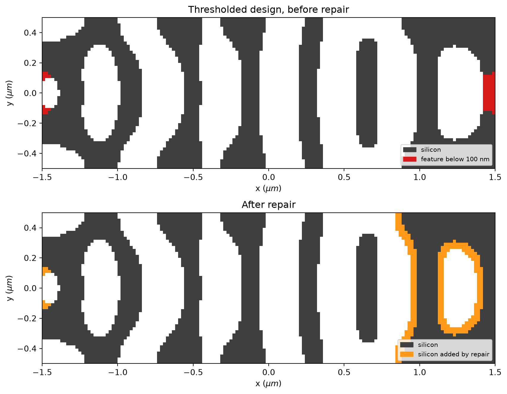
Verification and GDS Export
We verify the final binary design with a broadband, high-accuracy simulation using a finer grid (min_steps_per_wvl=30 and a 10 nm design-region mesh) and a FieldMonitor to inspect the mirror in action.
ldas = np.linspace(1.50, 1.60, 21)
freqs = td.C_0 / ldas
base = make_sim_base(msw=30, override_dl=(0.01, 0.01, 0.02), freqs=freqs, with_field=True)
eps_final = eps_sio2 + (eps_si - eps_sio2) * design.astype(float)
sim_verify = base.updated_copy(structures=[*base.structures, make_design_structure(eps_final)])

sim_data = web.run(sim_verify, task_name="reflector_verify", path="data/reflector_verify.hdf5")
11:21:38 UTC Created task 'reflector_verify' with resource_id 'fdve-537f31d8-e7aa-40f2-817b-0ce8c8ac5cbf' and task_type 'FDTD'.
             View task using web UI at
             'https://tidy3d.simulation.cloud/workbench?taskId=fdve-537f31d8-e7a
             a-40f2-817b-0ce8c8ac5cbf'.
Task folder: 'default'.
11:21:40 UTC Estimated FlexCredit cost: 0.065. This assumes the FDTD solver runs
             for the full simulation time; if early shutoff is reached, the
             billed cost can be lower. Use 'web.real_cost(task_id)' to get the
             billed FlexCredit cost after a simulation run.
status = queued
             To cancel the simulation, use 'web.abort(task_id)' or
             'web.delete(task_id)' or abort/delete the task in the web UI.
             Terminating the Python script will not stop the job running on the
             cloud.
11:21:55 UTC starting up solver
running solver
11:22:03 UTC early shutoff detected at 29%, exiting.
status = postprocess
11:22:04 UTC status = success
11:22:06 UTC View simulation result at
             'https://tidy3d.simulation.cloud/workbench?taskId=fdve-537f31d8-e7a
             a-40f2-817b-0ce8c8ac5cbf'.
11:22:07 UTC Loading results from data/reflector_verify.hdf5
The reflection spectrum stays high across the full band, and the field map shows the incident mode turned around within the first few teeth of the mirror.
R = np.abs(sim_data["refl"].amps.sel(direction="-", mode_index=0).values) ** 2

fig, (ax1, ax2) = plt.subplots(1, 2, figsize=(13, 4), tight_layout=True)
ax1.plot(ldas, 10 * np.log10(R), "-o")
ax1.set_xlabel(r"Wavelength ($\mu m$)")
ax1.set_ylabel("Reflection (dB)")
ax1.grid()
sim_data.plot_field(field_monitor_name="field", field_name="E", val="abs^2", f=freq0, ax=ax2)
plt.show()

i0 = np.argmin(np.abs(ldas - lda0))
print(f"R(1550 nm) = {100 * R[i0]:.2f}%")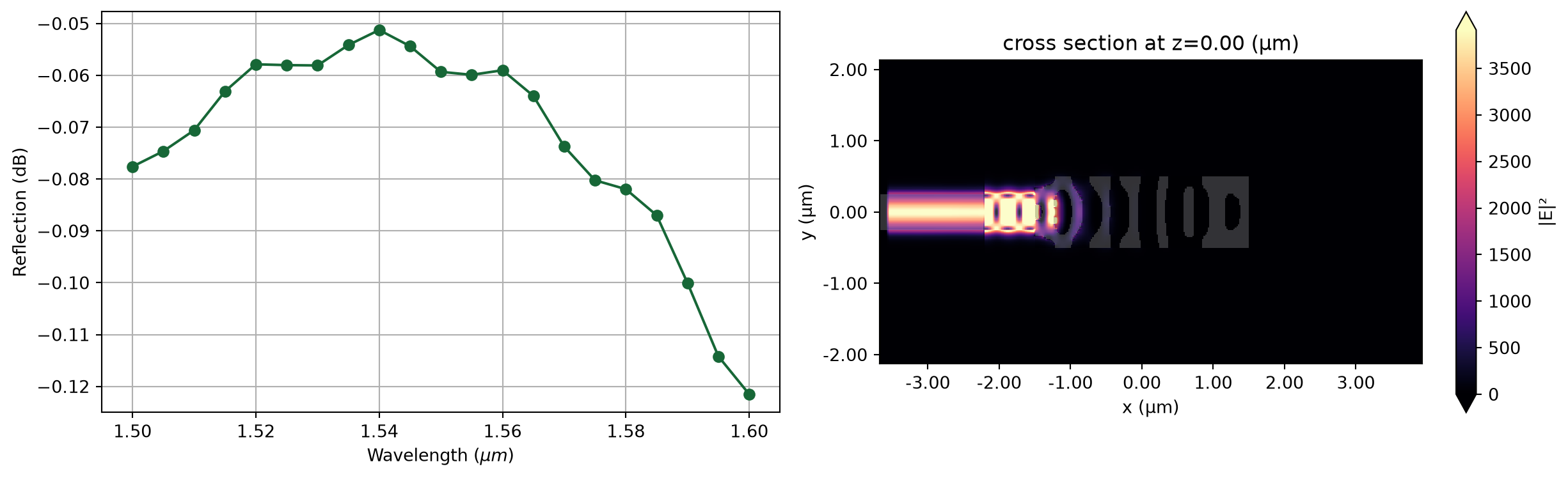
R(1550 nm) = 98.64%Finally, we export the design to GDS directly on layer (1, 0), where the SiEPIC PDK expects the silicon geometry.
eps_final = eps_sio2 + (eps_si - eps_sio2) * design.astype(float)
sim_export = make_sim_base().updated_copy(
    structures=[*make_sim_base().structures, make_design_structure(eps_final)]
)
layer_map = {structure.medium: (1, 0) for structure in sim_export.structures}
sim_export.to_gds_file(
    fname="reflector.gds", z=0, permittivity_threshold=(eps_sio2 + eps_si) / 2, frequency=freq0,
    gds_layer_dtype_map=layer_map, gds_cell_name="REFLECTOR",
)
Fabry-Perot Cavity Circuit on the SiEPIC PDK
We now assemble the cavity circuit with PhotonForge using the SiEPIC OpenEBL technology. The reflector GDS becomes a component with one optical port and a Tidy3D S-matrix model. Two mirrors terminate a cavity waveguide that is side-coupled to a bus through an adiabatic S-bend coupler. The circuit is referenced at its two bus ports, so the simulation captures the pure device physics; the fiber interface is added later as layout only.
import photonforge as pf
import siepic_forge as siepic

pf.config.default_technology = siepic.ebeam()

gap = 0.20              # coupling gap (um)
coupling_length = 6.0
arm_length = 15.0

reflector = pf.find_top_level(*pf.load_layout("reflector.gds").values())[0]
reflector.name = "REFLECTOR"
reflector.add_port(pf.Port((reflector.bounds()[0][0], 0.0), 0, "TE_1550_500"), port_name="P0")
reflector.add_model(pf.Tidy3DModel(symmetry=(0, -1, 0), verbose=False), "Tidy3D")

coupler = pf.parametric.s_bend_straight_coupler(
    port_spec="TE_1550_500", coupling_distance=gap + wg_width, coupling_length=coupling_length,
    s_bend_length=10.0, s_bend_offset=2.0, euler_fraction=0.5,
)
arm = pf.parametric.straight(port_spec="TE_1550_500", length=arm_length)

ports = dict(coupler.ports)
cav_l, cav_r = sorted((n for n, p in ports.items() if abs(p.center[1]) < 0.2), key=lambda n: ports[n].center[0])
bus_l, bus_r = sorted((n for n, p in ports.items() if abs(p.center[1]) >= 0.2), key=lambda n: ports[n].center[0])

fp = pf.Component("FP_CAVITY")
coup = fp.add_reference(coupler)
arm_l, arm_r = fp.add_reference(arm), fp.add_reference(arm)
refl_l, refl_r = fp.add_reference(reflector), fp.add_reference(reflector)
arm_l.connect("P1", coup[cav_l])
refl_l.connect("P0", arm_l["P0"])
arm_r.connect("P0", coup[cav_r])
refl_r.connect("P0", arm_r["P1"])
fp.add_port(coup[bus_l], port_name="P0")
fp.add_port(coup[bus_r], port_name="P1")
fp.add_model(pf.CircuitModel(verbose=False), "Circuit")'Circuit'The circuit S-matrix composes Tidy3D-computed S-matrices of the mirror and coupler with analytic waveguide models for the straight arms. On resonance, the side-coupled standing-wave cavity reflects the light back along the bus, so transmission dips and reflection peaks together.
wl_sweep = np.linspace(1.540, 1.560, 601)
s = fp.s_matrix(
    td.C_0 / wl_sweep,
    show_progress=False,
    model_kwargs={"verbose": False},
)
wl = td.C_0 / np.array(s.frequencies) * 1e3
order = np.argsort(wl)
T = np.abs(np.array(s.elements[("P0@0", "P1@0")]))[order] ** 2
R_bus = np.abs(np.array(s.elements[("P0@0", "P0@0")]))[order] ** 2
wl = wl[order]

dips = [i for i in range(1, len(T) - 1) if T[i] < T[i - 1] and T[i] < T[i + 1] and T[i] < 0.5 * np.median(T)]
print("resonances (nm):", np.round(wl[dips], 2))
print("FSR (nm):", np.round(np.diff(wl[dips]), 2))

plt.figure(figsize=(9, 4.5))
plt.plot(wl, 10 * np.log10(np.maximum(T, 1e-12)), label="$|S_{21}|^2$")
plt.plot(wl, 10 * np.log10(np.maximum(R_bus, 1e-12)), alpha=0.8, label="$|S_{11}|^2$")
plt.xlabel("Wavelength (nm)")
plt.ylabel("Power (dB)")
plt.legend()
plt.grid()
plt.tight_layout()
plt.show()
11:22:11 UTC WARNING: Structure at 'structures[13]' has bounds that extend exactly to simulation edges. This can cause unexpected behavior. If intending to extend the structure to infinity along one dimension, use td.inf as a size variable instead to make this explicit.
WARNING: Suppressed 1 WARNING message.
             WARNING: Structure at 'structures[13]' has bounds that extend
             exactly to simulation edges. This can cause unexpected behavior. If
             intending to extend the structure to infinity along one dimension,
             use td.inf as a size variable instead to make this explicit.
WARNING: Suppressed 1 WARNING message.
             WARNING: Structure at 'structures[13]' has bounds that extend
             exactly to simulation edges. This can cause unexpected behavior. If
             intending to extend the structure to infinity along one dimension,
             use td.inf as a size variable instead to make this explicit.
WARNING: Suppressed 1 WARNING message.
             WARNING: Structure at 'structures[13]' has bounds that extend
             exactly to simulation edges. This can cause unexpected behavior. If
             intending to extend the structure to infinity along one dimension,
             use td.inf as a size variable instead to make this explicit.
WARNING: Suppressed 1 WARNING message.
             WARNING: Structure at 'structures[13]' has bounds that extend
             exactly to simulation edges. This can cause unexpected behavior. If
             intending to extend the structure to infinity along one dimension,
             use td.inf as a size variable instead to make this explicit.
             WARNING: Structure at 'structures[14]' has bounds that extend
             exactly to simulation edges. This can cause unexpected behavior. If
             intending to extend the structure to infinity along one dimension,
             use td.inf as a size variable instead to make this explicit.
             WARNING: Structure at 'structures[13]' has bounds that extend
             exactly to simulation edges. This can cause unexpected behavior. If
             intending to extend the structure to infinity along one dimension,
             use td.inf as a size variable instead to make this explicit.
WARNING: Suppressed 1 WARNING message.
11:23:59 UTC WARNING: Structure at 'structures[13]' has bounds that extend
             exactly to simulation edges. This can cause unexpected behavior. If
             intending to extend the structure to infinity along one dimension,
             use td.inf as a size variable instead to make this explicit.
WARNING: Suppressed 1 WARNING message.
             WARNING: Warning messages were found in the solver log. For more
             information, check 'SimulationData.log' or use
             'web.download_log(task_id)'.
resonances (nm): [1543.57 1548.3  1553.03 1557.8 ]
FSR (nm): [4.73 4.73 4.77]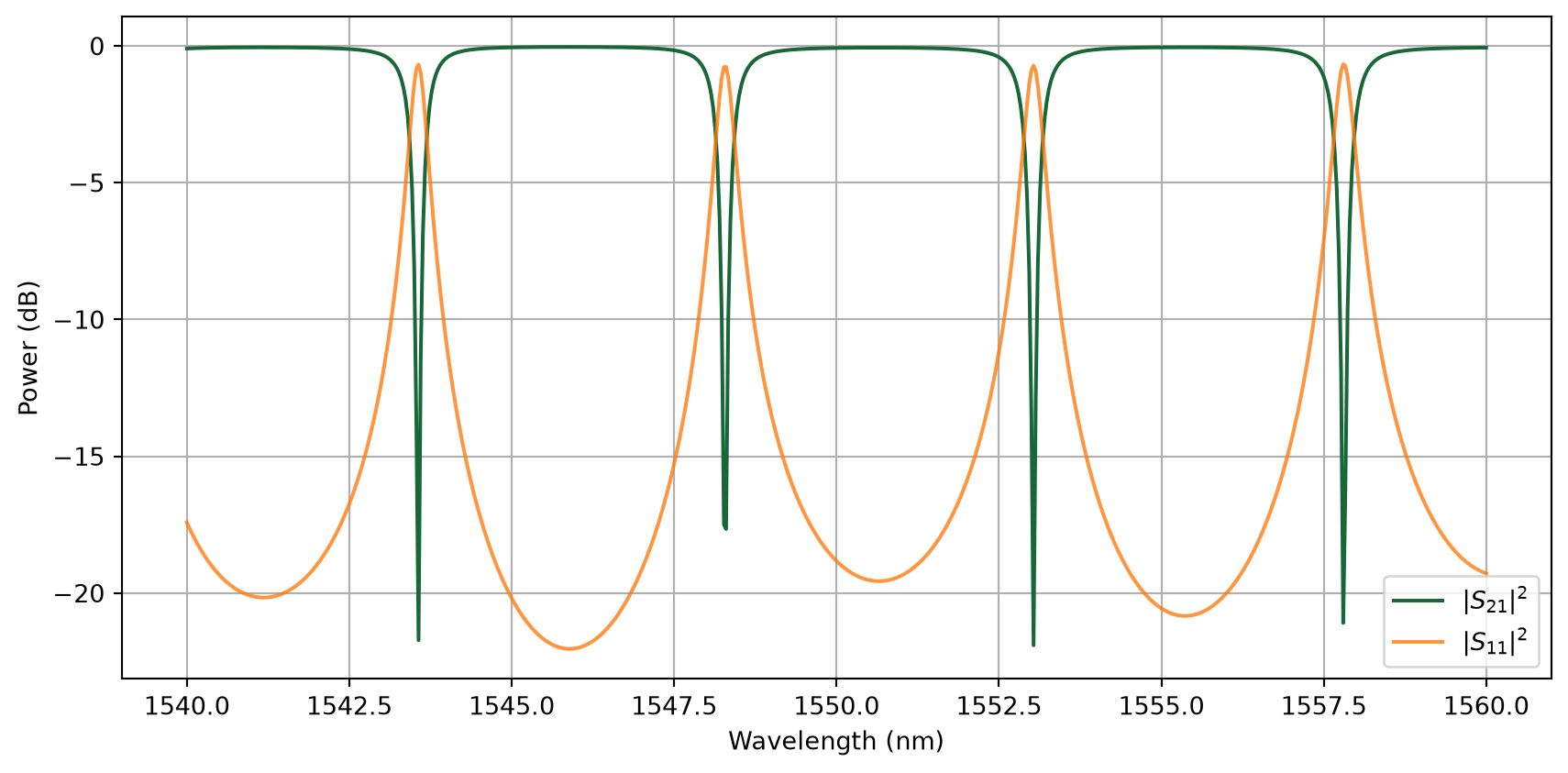
Quality Factor
To determine the loaded quality factor we rescan the central resonance with 5 pm resolution and read the full width at half maximum from the interpolated half-max crossings, using the window edge as the baseline (the median would sit on the Lorentzian wings and bias the width).
def fwhm_from_dip(wl_nm, T_lin):
    """Resonance center, FWHM (nm) and loaded Q from interpolated half-max crossings."""
    i = int(np.argmin(T_lin))
    half = (T_lin.max() + T_lin[i]) / 2
    left = right = None
    for j in range(i, 0, -1):
        if T_lin[j - 1] >= half > T_lin[j]:
            left = np.interp(half, [T_lin[j], T_lin[j - 1]], [wl_nm[j], wl_nm[j - 1]])
            break
    for j in range(i, len(T_lin) - 1):
        if T_lin[j + 1] >= half > T_lin[j]:
            right = np.interp(half, [T_lin[j], T_lin[j + 1]], [wl_nm[j], wl_nm[j + 1]])
            break
    lam0, fwhm = (left + right) / 2, right - left
    return lam0, fwhm, lam0 / fwhm


lam_c = wl[dips[len(dips) // 2]] / 1e3
wl_fine = np.linspace(lam_c - 0.0012, lam_c + 0.0012, 481)
s_fine = fp.s_matrix(
    td.C_0 / wl_fine,
    show_progress=False,
    model_kwargs={"verbose": False},
)
wlf = td.C_0 / np.array(s_fine.frequencies) * 1e3
order = np.argsort(wlf)
Tf = np.abs(np.array(s_fine.elements[("P0@0", "P1@0")]))[order] ** 2
wlf = wlf[order]

lam0, fwhm, Q = fwhm_from_dip(wlf, Tf)
print(f"resonance = {lam0:.3f} nm, FWHM = {fwhm * 1e3:.0f} pm, loaded Q = {Q:.0f}")

plt.figure(figsize=(8.5, 4.5))
plt.plot(wlf, 10 * np.log10(Tf), "o", ms=3, alpha=0.6)
plt.axvspan(lam0 - fwhm / 2, lam0 + fwhm / 2, alpha=0.15, color="orange", label=f"FWHM = {fwhm*1e3:.0f} pm, Q = {Q:.0f}")
plt.xlabel("Wavelength (nm)")
plt.ylabel("Transmission (dB)")
plt.legend()
plt.grid()
plt.tight_layout()
plt.show()
11:24:49 UTC WARNING: Structure at 'structures[13]' has bounds that extend exactly to simulation edges. This can cause unexpected behavior. If intending to extend the structure to infinity along one dimension, use td.inf as a size variable instead to make this explicit.
WARNING: Suppressed 1 WARNING message.
             WARNING: Structure at 'structures[13]' has bounds that extend
             exactly to simulation edges. This can cause unexpected behavior. If
             intending to extend the structure to infinity along one dimension,
             use td.inf as a size variable instead to make this explicit.
WARNING: Suppressed 1 WARNING message.
             WARNING: Structure at 'structures[13]' has bounds that extend
             exactly to simulation edges. This can cause unexpected behavior. If
             intending to extend the structure to infinity along one dimension,
             use td.inf as a size variable instead to make this explicit.
WARNING: Suppressed 1 WARNING message.
11:24:50 UTC WARNING: Structure at 'structures[13]' has bounds that extend
             exactly to simulation edges. This can cause unexpected behavior. If
             intending to extend the structure to infinity along one dimension,
             use td.inf as a size variable instead to make this explicit.
WARNING: Suppressed 1 WARNING message.
             WARNING: Structure at 'structures[13]' has bounds that extend
             exactly to simulation edges. This can cause unexpected behavior. If
             intending to extend the structure to infinity along one dimension,
             use td.inf as a size variable instead to make this explicit.
             WARNING: Structure at 'structures[14]' has bounds that extend
             exactly to simulation edges. This can cause unexpected behavior. If
             intending to extend the structure to infinity along one dimension,
             use td.inf as a size variable instead to make this explicit.
             WARNING: Structure at 'structures[13]' has bounds that extend
             exactly to simulation edges. This can cause unexpected behavior. If
             intending to extend the structure to infinity along one dimension,
             use td.inf as a size variable instead to make this explicit.
WARNING: Suppressed 1 WARNING message.
11:26:14 UTC WARNING: Structure at 'structures[13]' has bounds that extend
             exactly to simulation edges. This can cause unexpected behavior. If
             intending to extend the structure to infinity along one dimension,
             use td.inf as a size variable instead to make this explicit.
WARNING: Suppressed 1 WARNING message.
             WARNING: Warning messages were found in the solver log. For more
             information, check 'SimulationData.log' or use
             'web.download_log(task_id)'.
resonance = 1553.069 nm, FWHM = 317 pm, loaded Q = 4900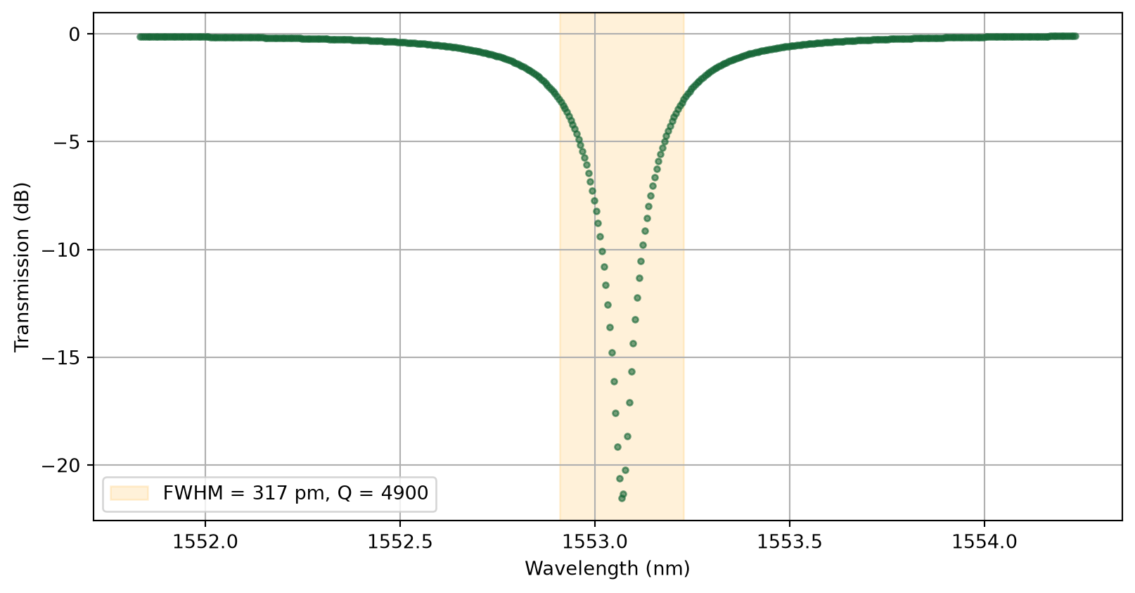
Fabrication-Ready Layout with Grating Couplers
For tapeout we attach two ebeam_gc_te1550 grating couplers from the SiEPIC library, placed by the SiEPIC conventions: a vertical fiber-array column at 127 \(\mu m\) pitch with an opt_in label on the Text (10, 0) layer for automated probing. The grating couplers serve as layout here and are not simulated. Rotating the cavity parallel to the coupler column keeps the routing to a single bend on each side.
gc_pitch = 127.0        # SiEPIC fiber-array pitch (um)
opt_in_label = "opt_in_TE_1550_device_FPcavity"

gc = siepic.component("ebeam_gc_te1550")
chip = pf.Component("FP_CHIP")
gc_in = chip.add_reference(gc)
gc_out = chip.add_reference(gc)
gc_out.translate((0, -gc_pitch))
fp_ref = chip.add_reference(fp)
fp_ref.rotate(-90)
fp_ref.translate((12.0, -30.0))
chip.add_reference(pf.parametric.route(port1=(gc_in, "P0"), port2=(fp_ref, "P0"), radius=5.0))
chip.add_reference(pf.parametric.route(port1=(fp_ref, "P1"), port2=(gc_out, "P0"), radius=5.0))

chip.add("Text", pf.Label(opt_in_label, tuple(np.array(gc_in["P1"].center)[:2]), anchor="W"))
pf.write_layout("fp_chip.gds", chip)
print("chip bounds:", chip.bounds())
chip bounds: (array([ -39.969, -140.5 ]), array([14.95 , 13.669]))Finally, we display the assembled chip for a last visual inspection before tapeout. PhotonForge components render natively in notebooks.
chip
To zoom into the cavity itself, we display the FP_CAVITY component, which shows the two inverse designed mirrors, the straight cavity arms, and the S-bend bus coupler in detail.
fp
The loaded quality factor of the cavity is set by the coupling gap rather than the mirrors: widening the gap trades extinction depth for a higher Q, while the inverse designed mirrors would support a mirror-limited finesse an order of magnitude beyond the loaded value measured here.
No matching results found.


 TERMS & CONDITIONS


 How the process works:
 Try this real URL to see an example: