





import gdstk
import matplotlib.pyplot as plt
import numpy as np
import tidy3d as td
import tidy3d.web as web
TIDY3D
LEARNING CENTER
Example Library

Waveguide to ring coupling
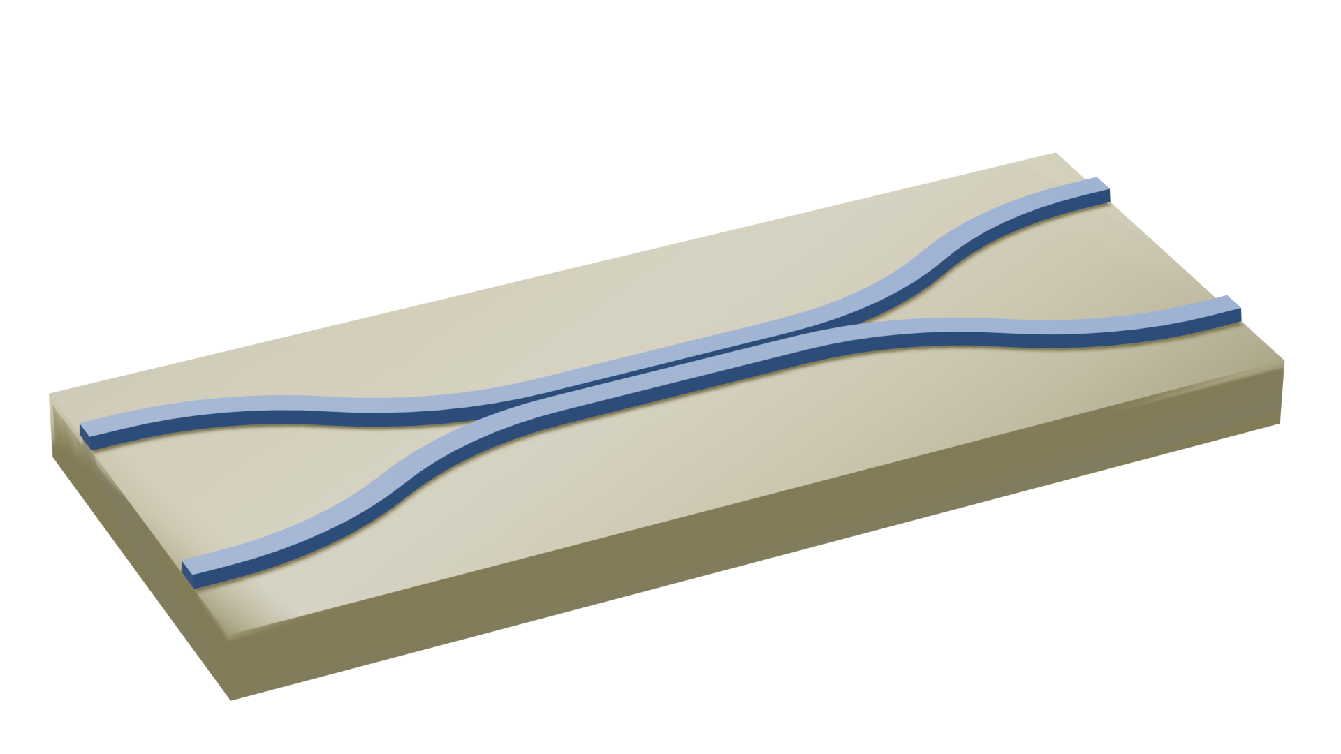
Optical ring resonators are key components in the field of integrated photonics. The unique capability of ring resonators to selectively interact with specific wavelengths of light makes them extremely versatile. They can be utilized in a broad array of applications, including optical filtering, modulating, switching, and sensing. However, simulating a ring resonator can be computationally expensive due to the high-Q resonances. Alternatively, we can investigate the coupling between a straight waveguide to a ring only by simulating the coupling region. The coupling coefficients can be extracted from this much simpler simulation.
Noticeably, in a waveguide-to-ring simulation, one of the simulation domain boundaries intersects the ring structure. Structures that are not translationally invariant inside a PML can make an FDTD simulation diverge. Tidy3D now enables extrude_structures=True by default for PML, so near-boundary structures are automatically extended through the PML to enforce translational invariance. This default avoids the divergence shown in older versions of this notebook, but it also changes the effective geometry inside the absorbing layer.
In this notebook, we first disable structure extrusion on the PML boundary that intersects the ring to reproduce the divergence mechanism. We then discuss the current default PML behavior and use an Absorber boundary as a conservative alternative for this curved geometry. The absorber functions similarly to PML by absorbing outgoing radiation to mimic infinite space. In standard (translationally invariant) setups, the absorber usually has slightly higher reflection and requires more computation than PML. However, it is numerically robust for slanted geometries, and does not require changing the structure into an extruded continuation inside the absorbing layer, which in itself can introduce numerical reflections.
FDTD simulations can diverge due to various reasons. If you run into any simulation divergence issues, please follow the steps outlined in our troubleshooting guide to resolve it. The same guide also discusses PML structure extrusion and its possible reflection artifacts in a simpler slanted-waveguide example.
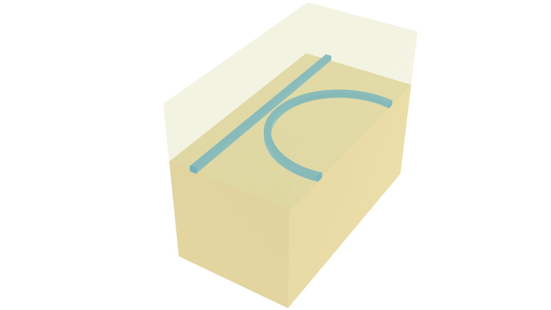
For more integrated photonic examples such as the 8-Channel mode and polarization de-multiplexer, the broadband bi-level taper polarization rotator-splitter, and the broadband directional coupler, please visit our examples page.
If you are new to the finite-difference time-domain (FDTD) method, we highly recommend going through our FDTD101 tutorials.
Simulation Setup
Define simulation wavelength range to be 1.5 \(\mu m\) to 1.6 \(\mu m\). .
lda0 = 1.55  # central wavelength
ldas = np.linspace(1.5, 1.6, 101)  # wavelength range of interest
freq0 = td.C_0 / lda0  # central frequency
freqs = td.C_0 / ldas  # frequency range of interest
fwidth = 0.5 * (np.max(freqs) - np.min(freqs))  # frequency width of the source
The ring and waveguide are made of silicon. The top and bottom claddings are made of silicon oxide. Here we use the materials from Tidy3D’s material library directly.
# define silicon and silicon dioxide media from the material library
si = td.material_library["cSi"]["Li1993_293K"]
sio2 = td.material_library["SiO2"]["Horiba"]
Define the geometric parameters. The waveguide is 500 nm wide and 220 nm thick. The ring has a radius of 5 \(\mu m\) and the gap size is 50 nm.
w = 0.5  # width of the waveguide
h_si = 0.22  # thickness of the silicon layer
gap = 0.05  # gap size between the waveguides and the ring
r = 5  # radius of the ring
inf_eff = 1e2  # effective infinity

# simulation domain size
Lx = 2 * r + 2 * lda0
Ly = r / 2 + gap + 2 * w + lda0
Lz = 9 * h_si
We only need to define two structures: a straight waveguide and a ring. Both are commonly used PIC components introduced in the demonstration notebook. We can simply copy the associated functions here and them use to define the structures quickly. Namely, we copy the straight_waveguide function and the ring_resonator function.
def straight_waveguide(x0, y0, z0, x1, y1, wg_width, wg_thickness, medium, sidewall_angle=0):
    """
    This function defines a straight strip waveguide and returns the tidy3d structure of it.

    Parameters
    ----------
    x0: x coordinate of the waveguide starting position (um)
    y0: y coordinate of the waveguide starting position (um)
    z0: z coordinate of the waveguide starting position (um)
    x1: x coordinate of the waveguide end position (um)
    y1: y coordinate of the waveguide end position (um)
    wg_width: width of the waveguide (um)
    wg_thickness: thickness of the waveguide (um)
    medium: medium of the waveguide
    sidewall_angle: side wall angle of the waveguide (rad)
    """

    cell = gdstk.Cell("waveguide")  # define a gds cell

    path = gdstk.RobustPath((x0, y0), wg_width, layer=1, datatype=0)  # define a path
    path.segment((x1, y1))

    cell.add(path)  # add path to the cell

    # define geometry from the gds cell
    wg_geo = td.PolySlab.from_gds(
        cell,
        gds_layer=1,
        axis=2,
        slab_bounds=(z0 - wg_thickness / 2, z0 + wg_thickness / 2),
        sidewall_angle=sidewall_angle,
    )

    # define tidy3d structure of the bend
    wg = td.Structure(geometry=wg_geo[0], medium=medium)

    return wg
def ring_resonator(
x0,
y0,
z0,
R,
wg_width,
wg_thickness,
medium,
sidewall_angle=0,
):
"""
This function defines a ring and returns the tidy3d structure of it.
Parameters
----------
x0: x coordinate of center of the ring (um)
y0: y coordinate of center of the ring (um)
z0: z coordinate of center of the ring (um)
R: radius of the ring (um)
wg_width: width of the waveguide (um)
wg_thickness: thickness of the waveguide (um)
medium: medium of the waveguide
sidewall_angle: side wall angle of the waveguide (rad)
"""
cell = gdstk.Cell("top") # define a gds cell
# define a path
path_top = gdstk.RobustPath(
(x0 + R, y0), wg_width - wg_thickness * np.tan(np.abs(sidewall_angle)), layer=1, datatype=0
)
path_top.arc(R, 0, np.pi) # make the top half of the ring
cell.add(path_top) # add path to the cell
# the reference plane depends on the sign of the sidewall_angle
if sidewall_angle >= 0:
reference_plane = "top"
else:
reference_plane = "bottom"
# define top half ring geometry
ring_top_geo = td.PolySlab.from_gds(
cell,
gds_layer=1,
axis=2,
slab_bounds=(z0 - wg_thickness / 2, z0 + wg_thickness / 2),
sidewall_angle=sidewall_angle,
reference_plane=reference_plane,
)
# similarly for the bottom half of the ring
cell = gdstk.Cell("bottom")
path_bottom = gdstk.RobustPath(
(x0 + R, y0), wg_width - wg_thickness * np.tan(np.abs(sidewall_angle)), layer=1, datatype=0
)
path_bottom.arc(R, 0, -np.pi)
cell.add(path_bottom)
ring_bottom_geo = td.PolySlab.from_gds(
cell,
gds_layer=1,
axis=2,
slab_bounds=(z0 - wg_thickness / 2, z0 + wg_thickness / 2),
sidewall_angle=sidewall_angle,
reference_plane=reference_plane,
)
# define ring structure
ring = td.Structure(
geometry=td.GeometryGroup(geometries=ring_bottom_geo + ring_top_geo), medium=medium
)
return ringUse the above functions to define the Structures.
# define straight waveguide
waveguide = straight_waveguide(
    x0=-inf_eff,
    y0=0,
    z0=0,
    x1=inf_eff,
    y1=0,
    wg_width=w,
    wg_thickness=h_si,
    medium=si,
    sidewall_angle=0,
)

# define ring
ring = ring_resonator(
    x0=0,
    y0=w + gap + r,
    z0=0,
    R=r,
    wg_width=w,
    wg_thickness=h_si,
    medium=si,
    sidewall_angle=0,
)
We will use a ModeSource to excite the straight waveguide using the fundamental TE mode. A ModeMonitor is placed at the through to measure the transmission. Another ModeMonitor is placed at the ring to measure the coupling to the ring. For the monitor at the ring, we need to properly set up angle_theta, angle_theta, bend_radius, and bend_axis in the ModeSpec as demonstrated in the tutorial. Finally, we add a FieldMonitor to help visualize the field distribution.
n_si = 3.47
# mode spec for the source
mode_spec_source = td.ModeSpec(num_modes=1, target_neff=n_si)
# mode spec for the through port
mode_spec_through = mode_spec_source
# angle of the mode at the ring
theta = np.pi / 4
# mode spec for the drop port at the ring
mode_spec_drop = td.ModeSpec(
    num_modes=1, target_neff=n_si, angle_theta=theta, bend_radius=r, bend_axis=1
)

# add a mode source as excitation
mode_source = td.ModeSource(
    center=(-r - lda0 / 4, 0, 0),
    size=(0, 6 * w, 6 * h_si),
    source_time=td.GaussianPulse(freq0=freq0, fwidth=fwidth),
    direction="+",
    mode_spec=mode_spec_source,
    mode_index=0,
)

# add a mode monitor behind the source to measure reflected power
mode_monitor_reflection = td.ModeMonitor(
    center=(-r - lda0 / 2, 0, 0),
    size=mode_source.size,
    freqs=freqs,
    mode_spec=mode_spec_through,
    name="reflection",
)

# add a mode monitor to measure transmission at the through port
mode_monitor_through = td.ModeMonitor(
    center=(r + lda0 / 4, 0, 0),
    size=mode_source.size,
    freqs=freqs,
    mode_spec=mode_spec_through,
    name="through",
)

# add a mode monitor to measure transmission at the drop port
mode_monitor_drop = td.ModeMonitor(
    center=(np.sin(theta) * r, w + gap + r - np.cos(theta) * r, 0),
    size=(6 * w, 0, 6 * h_si),
    freqs=freqs,
    mode_spec=mode_spec_drop,
    name="drop",
)

# add a field monitor to visualize the field distribution
field_monitor = td.FieldMonitor(
    center=(0, 0, 0), size=(td.inf, td.inf, 0), freqs=[freq0], name="field"
)
PML Boundary with Structure Extrusion Disabled
First, we define the simulation with a PML on each side, but explicitly set extrude_structures=False on the positive \(y\) boundary where the ring intersects the simulation domain boundary. This reproduces the unstable setup that would have been obtained from the old PML default.
run_time = 2e-12  # simulation run time

# construct simulation
sim_pml_no_extrusion = td.Simulation(
    center=(0, Ly / 4, 0),
    size=(Lx, Ly, Lz),
    grid_spec=td.GridSpec.auto(min_steps_per_wvl=25, wavelength=lda0),
    structures=[waveguide, ring],
    sources=[mode_source],
    monitors=[
        mode_monitor_reflection,
        mode_monitor_through,
        mode_monitor_drop,
        field_monitor,
    ],
    run_time=run_time,
    boundary_spec=td.BoundarySpec(
        x=td.Boundary.pml(),
        y=td.Boundary(plus=td.PML(extrude_structures=False), minus=td.PML()),
        z=td.Boundary.pml(),
    ),
    medium=sio2,
    symmetry=(0, 0, 1),
)

# plot simulation
sim_pml_no_extrusion.plot(z=0)
plt.show()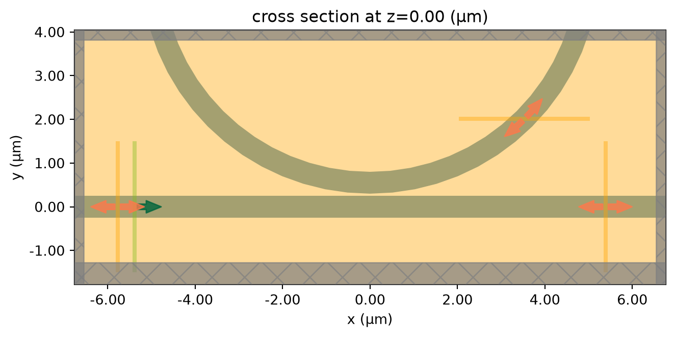
Submit the simulation to the server to run.
sim_data_pml_no_extrusion = web.run(
    simulation=sim_pml_no_extrusion,
    task_name="waveguide_to_ring_pml_no_extrusion",
    path="data/simulation_data_pml_no_extrusion.hdf5",
)
print(f"Simulation diverged: {sim_data_pml_no_extrusion.diverged}")
08:09:47 UTC Created task 'waveguide_to_ring_pml_no_extrusion' with resource_id 'fdve-d9d274b1-cb7a-4c6c-8f23-0a4925752ab9' and task_type 'FDTD'.
             View task using web UI at
             'https://tidy3d.simulation.cloud/workbench?taskId=fdve-d9d274b1-cb7
             a-4c6c-8f23-0a4925752ab9'.
Task folder: 'default'.
08:09:48 UTC Estimated FlexCredit cost: 0.623. This assumes the FDTD solver runs
             for the full simulation time; if early shutoff is reached, the
             billed cost can be lower. Use 'web.real_cost(task_id)' to get the
             billed FlexCredit cost after a simulation run.
08:09:50 UTC status = queued
             To cancel the simulation, use 'web.abort(task_id)' or
             'web.delete(task_id)' or abort/delete the task in the web UI.
             Terminating the Python script will not stop the job running on the
             cloud.
08:10:04 UTC starting up solver
08:10:05 UTC running solver
08:10:31 UTC early shutoff detected at 52%, exiting.
status = postprocess
08:10:34 UTC status = diverged
08:10:36 UTC View simulation result at
             'https://tidy3d.simulation.cloud/workbench?taskId=fdve-d9d274b1-cb7
             a-4c6c-8f23-0a4925752ab9'.
08:10:38 UTC Loading results from data/simulation_data_pml_no_extrusion.hdf5
             WARNING: The simulation has diverged! For more information, check
             'SimulationData.log' or use 'web.download_log(task_id)'.
Simulation diverged: TrueNow we see that the status of the job is shown to be diverged. This is expected because we intentionally disabled structure extrusion on the positive \(y\) PML boundary. The ring section in that PML layer is not perpendicular to the boundary and is not translationally invariant, as shown in the zoomed-in plot below. We are also given a warning about the divergence and prompted to check the log for more information.
print(sim_data_pml_no_extrusion.log)[08:10:00] USER: Simulation domain Nx, Ny, Nz: [759, 280, 82]
USER: Applied symmetries: (0, 0, 1)
USER: Number of computational grid points: 9.2279e+06.
USER: Subpixel averaging method: SubpixelSpec()
USER: Number of time steps: 6.2950e+04
USER: Automatic shutoff factor: 1.00e-05
USER: Time step (s): 3.1772e-17
USER:
[08:10:01] USER: Compute source modes time (s): 0.6339
USER: Rest of setup time (s): 0.3245
[08:10:22] USER: Compute monitor modes time (s): 16.8267
[08:10:28] USER: Solver time (s): 25.0910
USER: Time-stepping speed (cells/s): 1.39e+10
WARNING: The simulation has diverged!
WARNING: Some structures were found to be spatially varying inside
the PML. Ensure that structures are translationally invariant in the
PML regions in the direction normal to the PML interface.
Alternatively, switching the PML to Absorber boundary should fix the
divergence.
WARNING: A dispersive medium inside the PML regions was detected,
which may be causing the divergence. Consider making the medium
non-dispersive, or fitting a different dispersive model for that
medium. Alternatively, switching the PML to Absorber boundary should
fix the divergence.
USER: Loading data for monitor reflection
USER: Loading data for monitor through
USER: Loading data for monitor drop
USER: Loading data for monitor field
[08:10:29] USER: Post-processing time (s): 0.3841
====== SOLVER LOG ======
Processing grid and structures...
Building FDTD update coefficients...
Potential divergence: dispersive medium into PML.
Potential divergence: structures are not translationally invariant inside PML.
Solver setup time (s): 3.1109
Running solver for 62950 time steps...
- Time step 2517 / time 8.00e-14s ( 4 % done), field decay: 1.00e+00
- Time step 5035 / time 1.60e-13s ( 8 % done), field decay: 1.00e+00
- Time step 7553 / time 2.40e-13s ( 12 % done), field decay: 9.94e-01
- Time step 10071 / time 3.20e-13s ( 16 % done), field decay: 8.67e-02
- Time step 12589 / time 4.00e-13s ( 20 % done), field decay: 8.13e-04
- Time step 15107 / time 4.80e-13s ( 24 % done), field decay: 1.00e+00
- Time step 17625 / time 5.60e-13s ( 28 % done), field decay: 1.00e+00
- Time step 20143 / time 6.40e-13s ( 32 % done), field decay: 1.00e+00
- Time step 22661 / time 7.20e-13s ( 36 % done), field decay: 1.00e+00
- Time step 25179 / time 8.00e-13s ( 40 % done), field decay: 1.00e+00
- Time step 27697 / time 8.80e-13s ( 44 % done), field decay: 1.00e+00
- Time step 30215 / time 9.60e-13s ( 48 % done), field decay: 1.00e+00
- Time step 32733 / time 1.04e-12s ( 52 % done), field decay: 1.00e+00
Field diverged at time step 32910 ( 52 % done), exiting solver.
Time-stepping time (s): 21.8477
Data write time (s): 0.1321
The log tells us that there are two potential causes of divergence in this simulation: the presence of dispersive materials in the PML, and the fact that the ring is not translationally invariant in the PML region. While both can cause divergence, our built-in silicon material model has been fit to perform well for straight waveguides entering the PML at telecommunication wavelengths. Thus, the more likely cause of the divergence is the ring geometry that is not translationally invariant in the PML when extrusion is disabled.
# zoom-in plot around the pml
ax = sim_pml_no_extrusion.plot(z=0)
ax.set_xlim(4, 5.5)
ax.set_ylim(3.5, 4.5)
plt.show()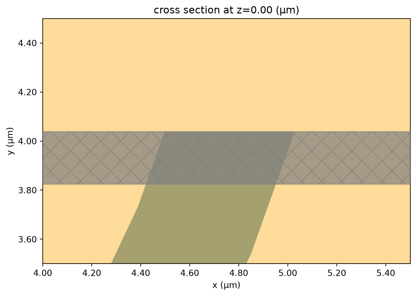
This can be further confirmed by plotting the electric field distribution. From the plot, we can see where the field built up and caused the simulation to diverge. As expected, the field built up around the ring and PML interface.
sim_data_pml_no_extrusion.plot_field(field_monitor_name="field", field_name="E", val="abs")
plt.show()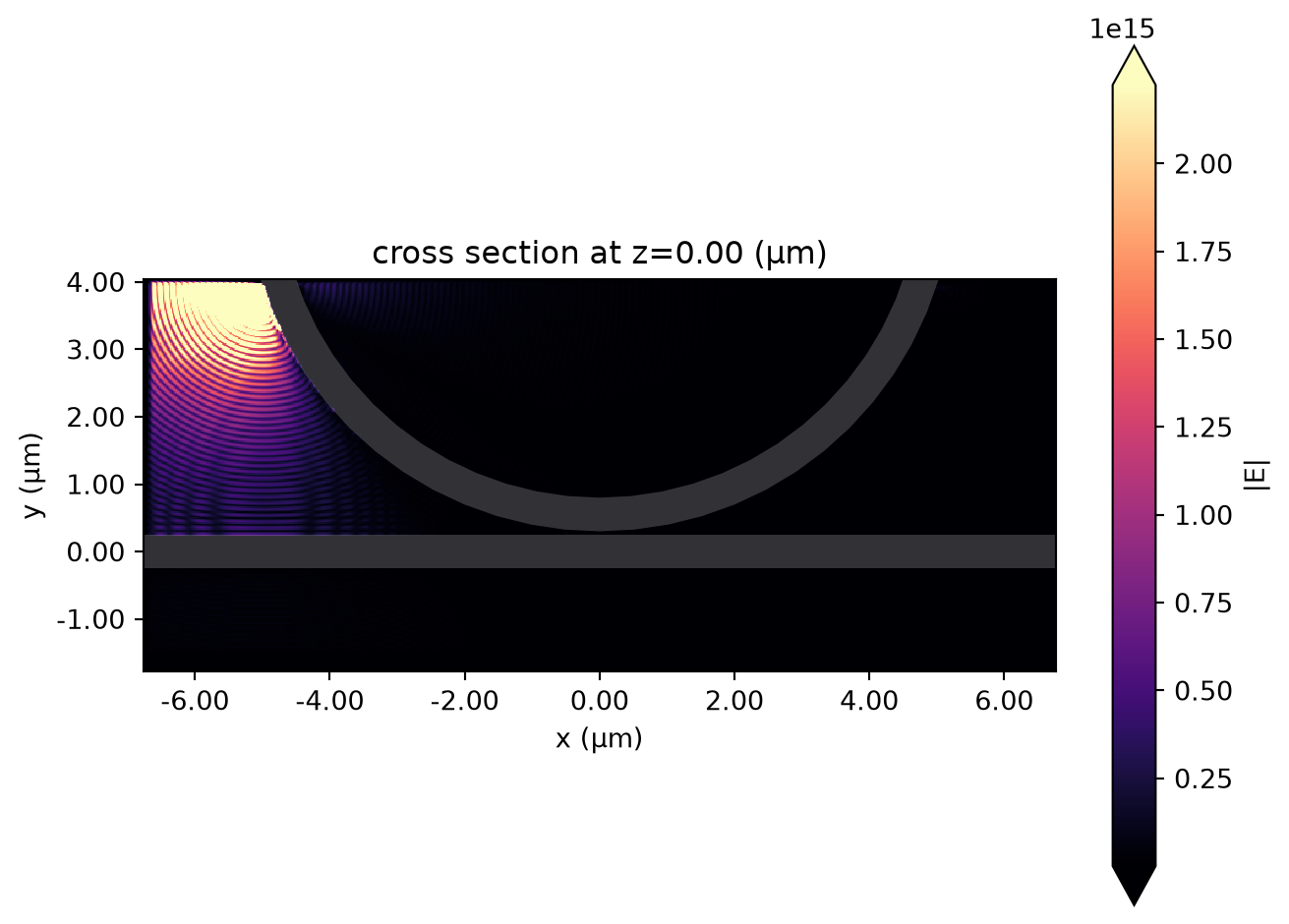
Default PML Boundary with Structure Extrusion
With the current default td.PML(), extrude_structures=True. If a structure is close enough to a PML boundary, Tidy3D automatically extends it through the PML along the direction normal to the boundary. This makes the material profile translationally invariant in the PML and prevents the divergence shown above.
This default is often the right choice when the structure physically should continue out of the simulation domain, such as a straight waveguide leaving the domain. However, it is not always a physically neutral operation. In this example, the original boundary intersects a curved ring; extrusion replaces the part of that curve inside the PML with an artificial continuation sampled from the material near the boundary. That artificial continuation can create unphysical reflections or phase errors even though the simulation remains numerically stable.
The runtime log is useful for detecting this situation: Tidy3D will warn that structure extrusion through PML boundaries overwrote original translational variance, which means the original geometry inside PML was not translationally invariant but extrusion made it invariant. We will run this default PML case and compare its reflected power against the absorber case below.
# Current default behavior on the problematic y+ PML boundary: structure extrusion is enabled.
sim_pml_extruded = sim_pml_no_extrusion.updated_copy(
    boundary_spec=sim_pml_no_extrusion.boundary_spec.updated_copy(
        y=sim_pml_no_extrusion.boundary_spec.y.updated_copy(plus=td.PML())
    )
)

sim_pml_extruded.boundary_spec.y.plus.extrude_structuresTrueSubmit the default PML simulation. This run should remain stable because the positive \(y\) PML now extrudes the ring structure through the absorbing layer.
sim_data_pml_extruded = web.run(
    simulation=sim_pml_extruded,
    task_name="waveguide_to_ring_pml_extruded",
    path="data/simulation_data_pml_extruded.hdf5",
)
print(f"Simulation diverged: {sim_data_pml_extruded.diverged}")
08:10:40 UTC Created task 'waveguide_to_ring_pml_extruded' with resource_id 'fdve-c45d671e-a51e-43ca-991d-010491aaeee1' and task_type 'FDTD'.
             View task using web UI at
             'https://tidy3d.simulation.cloud/workbench?taskId=fdve-c45d671e-a51
             e-43ca-991d-010491aaeee1'.
Task folder: 'default'.
08:10:41 UTC Estimated FlexCredit cost: 0.623. This assumes the FDTD solver runs
             for the full simulation time; if early shutoff is reached, the
             billed cost can be lower. Use 'web.real_cost(task_id)' to get the
             billed FlexCredit cost after a simulation run.
08:10:42 UTC status = queued
             To cancel the simulation, use 'web.abort(task_id)' or
             'web.delete(task_id)' or abort/delete the task in the web UI.
             Terminating the Python script will not stop the job running on the
             cloud.
08:10:50 UTC status = preprocess
08:10:54 UTC starting up solver
08:10:55 UTC running solver
08:11:14 UTC early shutoff detected at 19%, exiting.
status = postprocess
08:11:22 UTC status = success
08:11:24 UTC View simulation result at
             'https://tidy3d.simulation.cloud/workbench?taskId=fdve-c45d671e-a51
             e-43ca-991d-010491aaeee1'.
08:11:26 UTC Loading results from data/simulation_data_pml_extruded.hdf5
             WARNING: Warning messages were found in the solver log. For more
             information, check 'SimulationData.log' or use
             'web.download_log(task_id)'.
Simulation diverged: FalseThe simulation finishes, but the log should still be inspected. A warning that structure extrusion overwrote translational variance is a sign that the stable PML result may include an artifact caused by the geometry change.
print(sim_data_pml_extruded.log)[08:10:49] USER: Simulation domain Nx, Ny, Nz: [759, 280, 82]
USER: Applied symmetries: (0, 0, 1)
USER: Number of computational grid points: 9.2279e+06.
USER: Subpixel averaging method: SubpixelSpec()
USER: Number of time steps: 6.2950e+04
USER: Automatic shutoff factor: 1.00e-05
USER: Time step (s): 3.1772e-17
USER:
USER: Compute source modes time (s): 0.7741
[08:10:50] USER: Rest of setup time (s): 0.4657
[08:11:12] USER: Compute monitor modes time (s): 20.2758
USER: Solver time (s): 6.3040
USER: Time-stepping speed (cells/s): 2.11e+10
WARNING: Structure extrusion through PML boundaries was detected to
have overwritten original translational variance. The original
geometry inside PML was not translationally invariant, but extrusion
clipping made it invariant. This may affect simulation accuracy if
original structure was slanted.
USER: Loading data for monitor reflection
[08:11:13] USER: Loading data for monitor through
[08:11:15] USER: Loading data for monitor drop
[08:11:16] USER: Loading data for monitor field
USER: Post-processing time (s): 4.0125
====== SOLVER LOG ======
Processing grid and structures...
Building FDTD update coefficients...
Potential divergence: dispersive medium into PML.
Solver setup time (s): 0.5841
Running solver for 62950 time steps...
- Time step 2517 / time 8.00e-14s ( 4 % done), field decay: 1.00e+00
- Time step 5035 / time 1.60e-13s ( 8 % done), field decay: 1.00e+00
- Time step 7553 / time 2.40e-13s ( 12 % done), field decay: 9.94e-01
- Time step 10071 / time 3.20e-13s ( 16 % done), field decay: 8.69e-02
- Time step 12400 / time 3.94e-13s ( 19 % done), field decay: 8.80e-06
Field decay smaller than shutoff factor, exiting solver.
Time-stepping time (s): 5.4234
Data write time (s): 0.2941
Using Absorber Boundary
For this geometry, switching the positive \(y\) boundary to Absorber is a conservative remedy. The absorber avoids the PML divergence without replacing the curved ring segment in the absorbing region by an extruded continuation. Since the ring only intersects the positive \(y\) boundary, we only need to apply the absorber there and can keep PML on the other sides.
In addition, we increased the number of layers in the Absorber to 60 to ensure sufficient absorption and minimal reflection.
# copy simulation and update boundary condition
sim_absorber = sim_pml_no_extrusion.updated_copy(
    boundary_spec=sim_pml_no_extrusion.boundary_spec.updated_copy(
        y=sim_pml_no_extrusion.boundary_spec.y.updated_copy(plus=td.Absorber(num_layers=60))
    )
)

# run simulation
sim_data_absorber = web.run(
    simulation=sim_absorber,
    task_name="waveguide_to_ring_absorber",
    path="data/simulation_data_absorber.hdf5",
)
print(f"Simulation diverged: {sim_data_absorber.diverged}")
Created task 'waveguide_to_ring_absorber' with resource_id 'fdve-b93ff726-53a0-46ad-aab6-337e6d8b5a85' and task_type 'FDTD'.
             View task using web UI at
             'https://tidy3d.simulation.cloud/workbench?taskId=fdve-b93ff726-53a
             0-46ad-aab6-337e6d8b5a85'.
Task folder: 'default'.
08:11:28 UTC Estimated FlexCredit cost: 0.674. This assumes the FDTD solver runs
             for the full simulation time; if early shutoff is reached, the
             billed cost can be lower. Use 'web.real_cost(task_id)' to get the
             billed FlexCredit cost after a simulation run.
08:11:29 UTC status = queued
             To cancel the simulation, use 'web.abort(task_id)' or
             'web.delete(task_id)' or abort/delete the task in the web UI.
             Terminating the Python script will not stop the job running on the
             cloud.
08:11:37 UTC status = preprocess
08:11:41 UTC starting up solver
running solver
08:12:02 UTC early shutoff detected at 19%, exiting.
08:12:03 UTC status = postprocess
08:12:08 UTC status = success
08:12:10 UTC View simulation result at
             'https://tidy3d.simulation.cloud/workbench?taskId=fdve-b93ff726-53a
             0-46ad-aab6-337e6d8b5a85'.
08:12:20 UTC Loading results from data/simulation_data_absorber.hdf5
Simulation diverged: FalseAfter switching to Absorber, the simulation does not run into the divergence issue anymore. We compare this absorber result with the default PML result to see whether automatic extrusion introduces a measurable artifact. The usual forward through and drop powers are a useful first check, but a more sensitive diagnostic is the power in the opposite direction at the ring drop monitor.
# extract mode amplitudes in the through port
t_pml = sim_data_pml_extruded["through"].amps.sel(mode_index=0, direction="+")
t_absorber = sim_data_absorber["through"].amps.sel(mode_index=0, direction="+")

# extract mode amplitudes in the drop port
k_pml = sim_data_pml_extruded["drop"].amps.sel(mode_index=0, direction="+")
k_absorber = sim_data_absorber["drop"].amps.sel(mode_index=0, direction="+")

through_pml = np.abs(t_pml) ** 2
through_absorber = np.abs(t_absorber) ** 2
drop_pml = np.abs(k_pml) ** 2
drop_absorber = np.abs(k_absorber) ** 2

fig, (ax1, ax2) = plt.subplots(1, 2, figsize=(11, 4), tight_layout=True)

ax1.plot(ldas, through_pml, "--", label="Through, PML extrusion")
ax1.plot(ldas, through_absorber, label="Through, absorber")
ax1.plot(ldas, drop_pml, "--", label="Drop, PML extrusion")
ax1.plot(ldas, drop_absorber, label="Drop, absorber")
ax1.set_xlabel(r"Wavelength ($\mu m$)")
ax1.set_ylabel("Transmission")
ax1.set_xlim(1.5, 1.6)
ax1.set_ylim(0, 1)
ax1.legend()

ax2.plot(ldas, through_pml - through_absorber, label="Through")
ax2.plot(ldas, drop_pml - drop_absorber, label="Drop")
ax2.axhline(0, color="k", linewidth=0.8)
ax2.set_xlabel(r"Wavelength ($\mu m$)")
ax2.set_ylabel("PML extrusion - absorber")
ax2.set_xlim(1.5, 1.6)
ax2.legend()

plt.show()

print(f"max |through difference|: {float(np.max(np.abs(through_pml - through_absorber))):.3e}")
print(f"max |drop difference|: {float(np.max(np.abs(drop_pml - drop_absorber))):.3e}")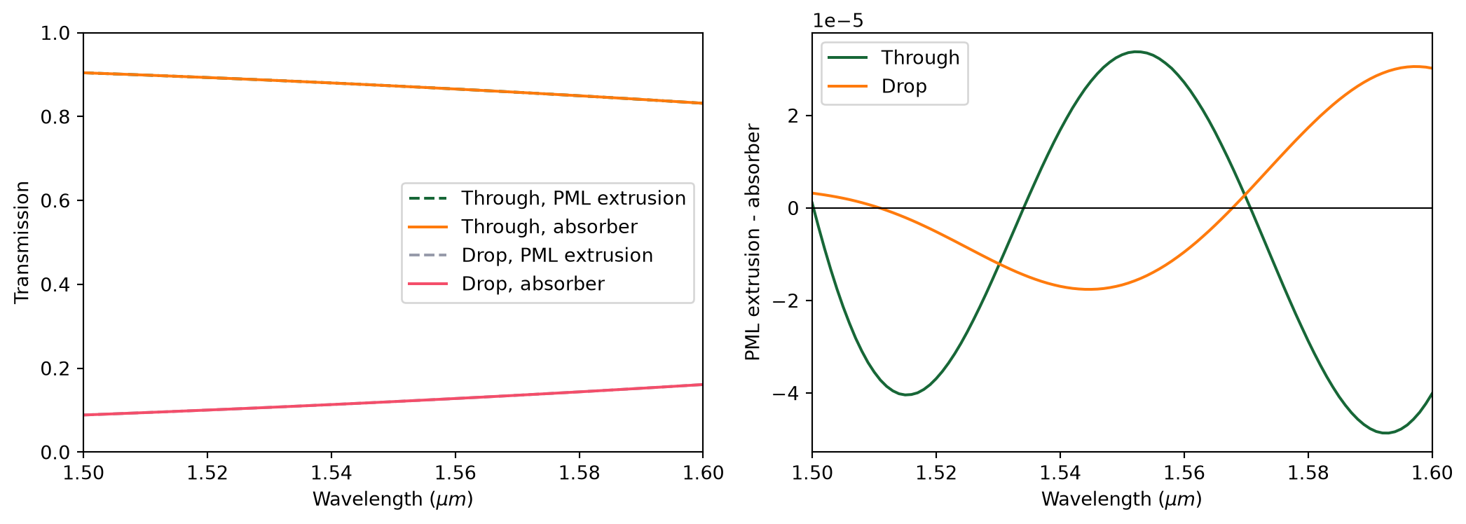
max |through difference|: 4.865e-05
max |drop difference|: 3.057e-05
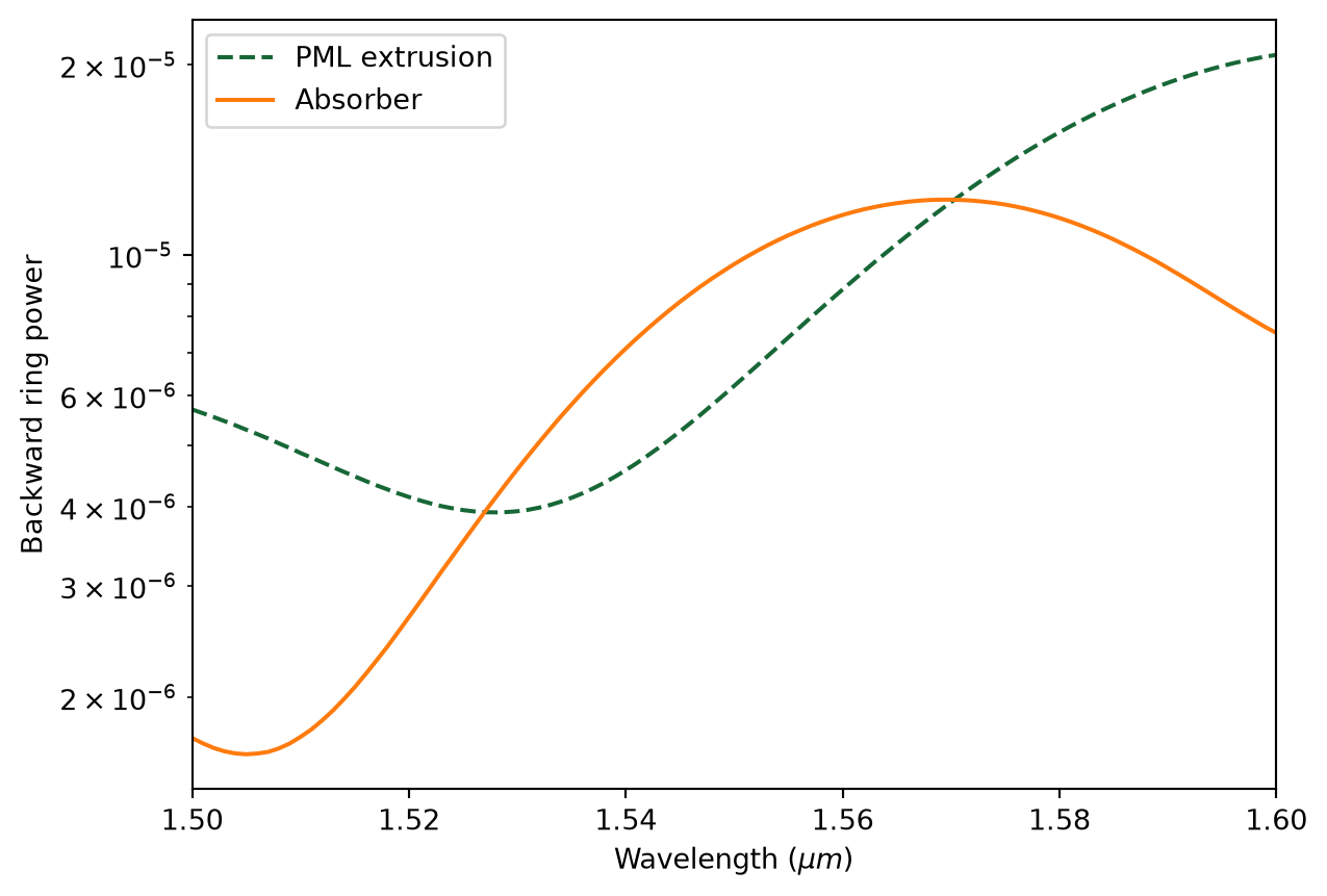
The forward through and drop spectra are nearly unchanged by the boundary choice. This means the main coupling quantities that this simulation with a truncated domain is designed to extract are not strongly affected by the PML extrusion in this setup. To look for a more subtle artifact from boundary reflection, we can use the drop monitor to measure the mode propagating in the opposite ring direction by selecting direction="-". In an ideal unidirectional coupling picture with no reflection caused by the boundary, this backward component should be zero.
drop_back_pml = sim_data_pml_extruded["drop"].amps.sel(mode_index=0, direction="-")
drop_back_absorber = sim_data_absorber["drop"].amps.sel(mode_index=0, direction="-")

drop_backward_pml = np.abs(drop_back_pml) ** 2
drop_backward_absorber = np.abs(drop_back_absorber) ** 2

plt.semilogy(ldas, drop_backward_pml, "--", label="PML extrusion")
plt.semilogy(ldas, drop_backward_absorber, label="Absorber")
plt.xlabel(r"Wavelength ($\mu m$)")
plt.ylabel("Backward ring power")
plt.xlim(1.5, 1.6)
plt.legend()
plt.show()

print(f"max backward drop power, PML extrusion: {float(drop_backward_pml.max()):.3e}")
print(f"max backward drop power, absorber: {float(drop_backward_absorber.max()):.3e}")
print(
    "max |backward drop power difference|: "
    f"{float(np.max(np.abs(drop_backward_pml - drop_backward_absorber))):.3e}"
)
max backward drop power, PML extrusion: 2.075e-05
max backward drop power, absorber: 1.225e-05
max |backward drop power difference|: 1.321e-05
The backward ring power is somewhat larger with PML extrusion than with the absorber. Its peak value is approximately 2.1e-5 for PML extrusion and 1.2e-5 for the absorber, compared with a forward drop power of about 1.6e-1. Thus this monitor detects a small difference between the boundary treatments that is not visible in the forward through and drop spectra. The effect is still very weak in absolute terms, but it is the clearest signature in this notebook of the artificial PML extrusion causing a small reflected ring component.
Finally, we visualize the field distribution for both stable simulations. The two interior fields are very similar for this setup. The absorber result remains the conservative choice when preserving the original curved boundary geometry is more important than the lower nominal reflection of PML, but the spectra above show that the PML extrusion artifact is limited to a weak backward ring component for this particular truncation.
fig, (ax1, ax2) = plt.subplots(1, 2, figsize=(10, 4), tight_layout=True)
sim_data_pml_extruded.plot_field(field_monitor_name="field", field_name="E", val="abs", ax=ax1)
sim_data_absorber.plot_field(field_monitor_name="field", field_name="E", val="abs", ax=ax2)
ax1.set_title("PML extrusion")
ax2.set_title("Absorber")
plt.show()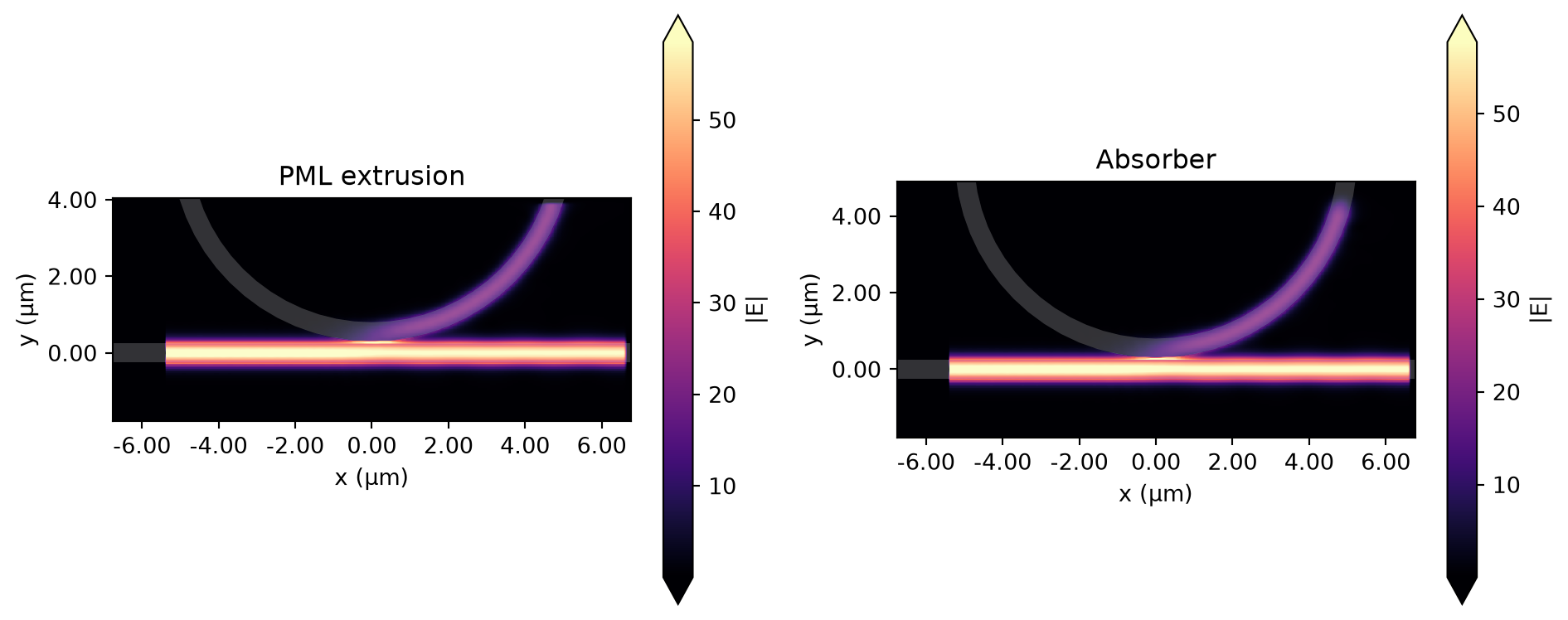
Absorber and PML Extrusion Tradeoffs
The best absorbing boundary depends on what should physically happen at the truncated edge of the simulation. Starting from Tidy3D version 2.11, the PML defaults with extrude_structures=True. This is usually preferable when the near-boundary structure should continue straight through the boundary, because it keeps the low reflection of PML while preventing material profiles inside the PML that are not translationally invariant. It is also the default, so many ordinary waveguide terminations work without extra boundary tuning. For a more direct slanted-waveguide illustration of the same tradeoff, see the diverged FDTD troubleshooting notebook.
Absorber is usually preferable when a structure intersects the boundary in a way that should not be automatically continued, as in this curved ring example. It preserves the original geometry at the cost of a thicker absorbing region and typically higher reflection than PML. In this particular simulation, the forward through/drop spectra and bus reflection from default PML extrusion and absorber are nearly indistinguishable. The backward drop monitor is more sensitive and shows a small excess ring-backward component for PML extrusion, but the magnitude is still too weak to change the extracted coupling spectra appreciably. That means the PML extrusion warning should be treated as a prompt to check the observables that matter for the model, not as proof that the result is inaccurate.
For absorbers, there are two possible sources of reflection. The first, and more common one, is that the ramping up of the conductivity is not sufficiently slow, which can be remedied by increasing the number of absorber layers (40 by default). The second one is that the absorption is not high enough, such that the light reaches the PEC boundary at the end of the absorber, travels back through it, and is still not fully attenuated before re-entering the simulation region. If this is the case, increasing the maximum conductivity (see the API reference) can help. In both cases, changing the order of the scaling of the conductivity (sigma_order) can also have an effect, but this is a more advanced setting that we typically do not recommend modifying.
No matching results found.


 TERMS & CONDITIONS

 How the process works:
 Try this real URL to see an example: