





Zhongpeng Sun, Harvard John A. Paulson School of Engineering and Applied Sciences
This notebook presents a Tidy3D supercell model of the hybrid BaTiO$_3$ (BTO)/TiO$_2$ electro-optic metasurface reported in Sun et al., arXiv:2608.00286.
We take as our starting point the transverse-electric (TE) guided-mode resonance near 1575 nm identified in the electrode-free unit-cell simulations presented in Supplementary Note 1 of the paper. Here, we investigate how this resonance is modified by the incorporation of gold interdigitated electrodes and how it responds to Pockels-induced changes in the BTO refractive index. To this end, we model and analyze the complete supercell, which comprises five TiO$_2$ nanopillars on an unetched BTO film between two adjacent electrodes.
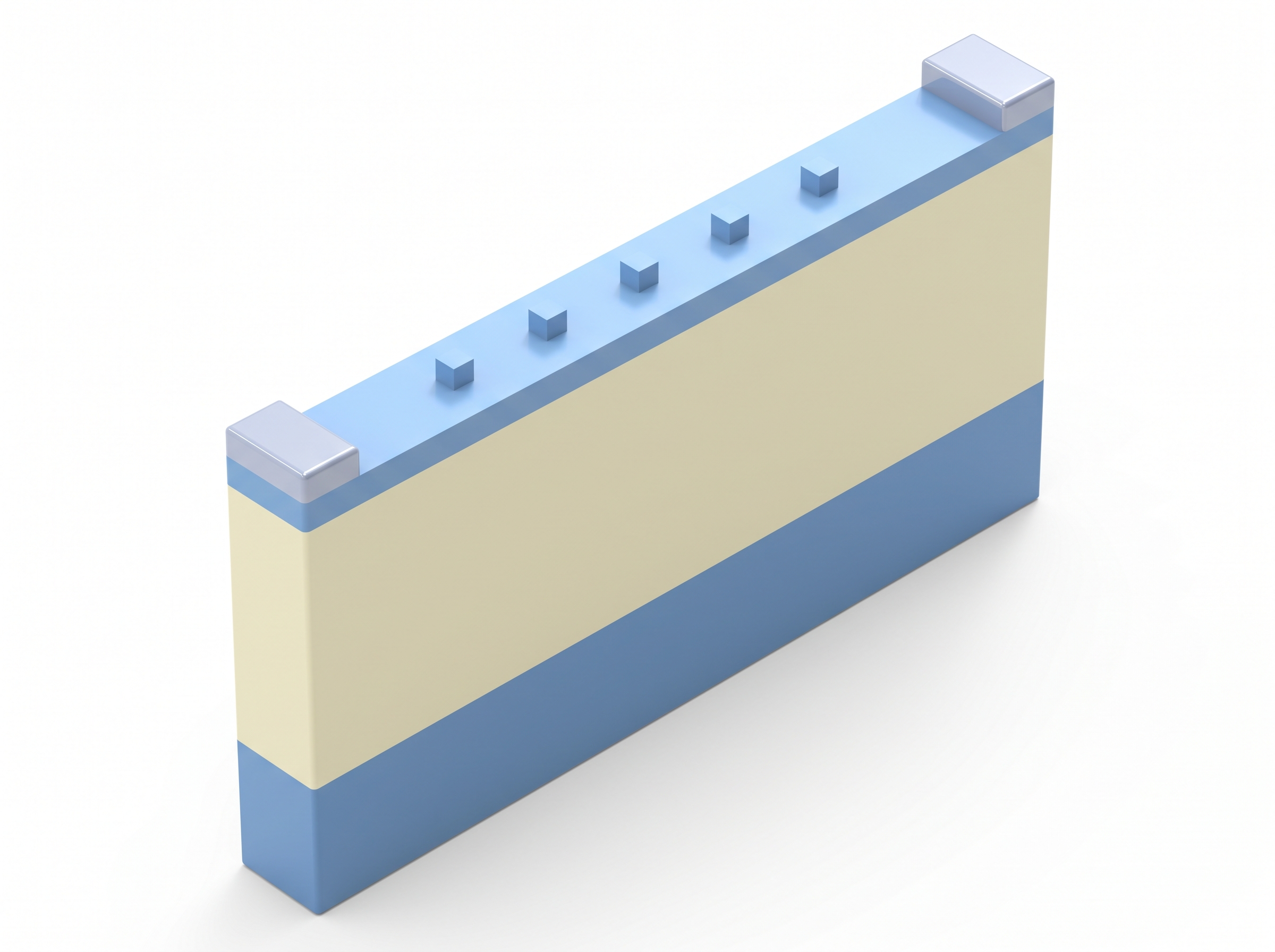
The notebook provides a reproducible workflow covering material fitting, device construction, spectral simulations at three applied voltages, automatic selection of the resonant-field wavelength, visualization of the $x$-$z$ field profile, and evaluation of the optical confinement factor.
What this notebook computes
-
Fits causal dispersive models to measured $n$-$k$ data for BTO, TiO$_2$, and SiO$_2$.
-
Applies the scalar Pockels perturbation used in the paper,
$$\Delta\!\left(\frac{1}{n_{\mathrm{BTO}}^2}\right) = r_{\mathrm{eff}}E_{\mathrm{DC}},$$
using the effective Pockels coefficient $r_{\mathrm{eff}}=130\ \mathrm{pm/V}$ and the DC field strength $E_{\mathrm{DC}}$ obtained from electrostatic simulations.
-
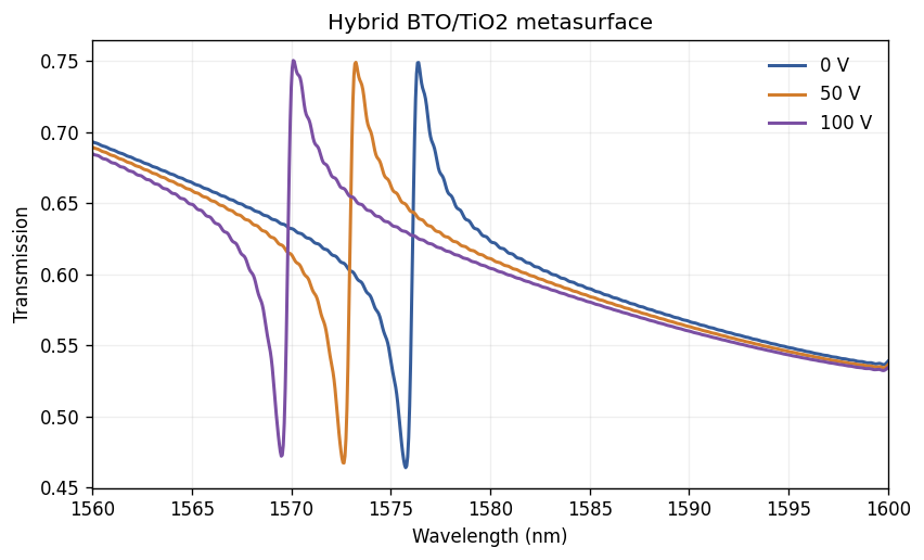
Simulates the complete device at 0, 50, and 100 V and displays the three absolute transmission spectra on a common plot.
-
Uses a lightweight line monitor in the BTO at 0 V to identify the wavelength with the largest spatially averaged $|E_x|^2$.
-
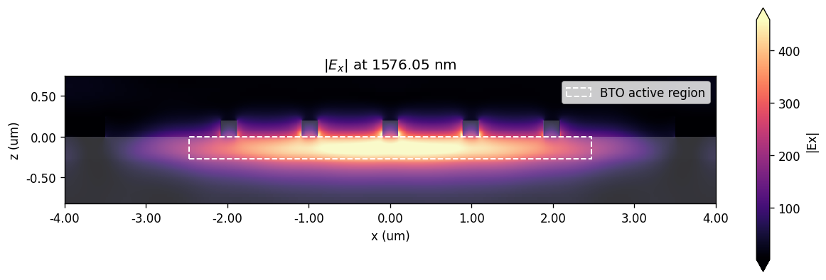
Runs a single-frequency field simulation at the selected wavelength, plots the $x$-$z$ cross-section through the nanopillar centers, and evaluates the active-region optical confinement factor.
%matplotlib inline

from pathlib import Path

import matplotlib.pyplot as plt
from matplotlib.patches import Rectangle
import numpy as np

import tidy3d as td
import tidy3d.web as web
from tidy3d.plugins.dispersion import FastDispersionFitter

plt.rcParams.update({"figure.dpi": 120, "axes.grid": False})
Simulation parameters
The wavelength sweep spans 1560–1600 nm with a step size of 0.05 nm, providing sufficient sampling to resolve the high-$Q$ guided-mode resonance. Electrostatic simulations give $E_{\mathrm{DC}}=6.92\ \mathrm{V/\mu m}$ at 50 V and $E_{\mathrm{DC}}=13.84\ \mathrm{V/\mu m}$ at 100 V. The DC field is assumed to scale linearly with the applied voltage.
# Units
um = 1.0
nm = 1e-3
pm = 1e-6

# Optical sweep
wavelength_nm = np.arange(1560.0, 1600.0 + 0.025, 0.05)
wavelength_um = wavelength_nm * nm
frequencies = td.C_0 / wavelength_um
design_wavelength = 1575 * nm

# Electro-optic model
voltages = (0.0, 50.0, 100.0)
r_eff = 130 * pm  # 130 pm/V, expressed in um/V
dc_field_per_volt = 6.92 / 50.0  # (V/um)/V
dc_fields = {voltage: dc_field_per_volt * voltage for voltage in voltages}

print(f"Spectral samples: {len(frequencies)}")
for voltage, field in dc_fields.items():
    print(f"{voltage:5.0f} V -> E_DC = {field:5.2f} V/um")
Spectral samples: 801
    0 V -> E_DC =  0.00 V/um
   50 V -> E_DC =  6.92 V/um
  100 V -> E_DC = 13.84 V/um
Dispersive materials and voltage-dependent BTO
The following material-data files are in the misc folder next to this notebook:
ALD_TiO2_90C_Cody_WithSiO2Native_um.txtBTOindex_um.txtSiO2underBTO_um.txt
Each file should be a header-free, three-column table containing wavelength (µm), $n$, and $k$. The measured data are fit to causal pole–residue models over 1.5–1.65 µm. Gold and crystalline silicon are described by the Johnson–Christy and lossless Palik models from the Tidy3D material library, respectively.
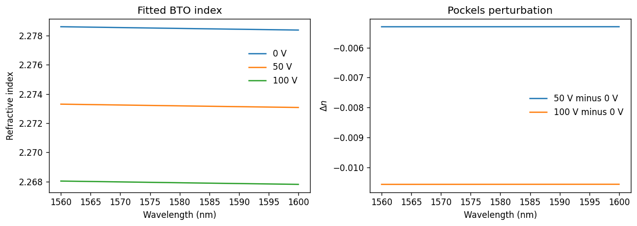
For each applied voltage, the Pockels-induced change is applied to the BTO index before the dispersive model is refit:
$$n(V)=\left[n(0)^{-2}+r_{\mathrm{eff}}E_{\mathrm{DC}}(V)\right]^{-1/2}.$$
A positive voltage therefore decreases the BTO refractive index and shifts the resonance toward shorter wavelengths, as reported in the paper. The extinction coefficient is assumed to remain unchanged.
To resolve the assigned electro-optic perturbation reliably, the RMS error of each BTO fit should be at least two orders of magnitude smaller than the corresponding voltage-induced index change.
In general, the Pockels effect must be described tensorially because different components of the applied DC field couple differently to each optical polarization through the electro-optic tensor. In the BTO layer of this device, however, both the applied DC field and the resonant optical electric field are almost entirely polarized along $x$. The response is therefore governed by a single effective electro-optic coefficient and can be reduced to the scalar relation above.
MATERIAL_DIR = Path("misc")

material_files = {
    "TiO2": MATERIAL_DIR / "ALD_TiO2_90C_Cody_WithSiO2Native_um.txt",
    "BTO": MATERIAL_DIR / "BTOindex_um.txt",
    "SiO2": MATERIAL_DIR / "SiO2underBTO_um.txt",
}

missing = [str(path) for path in material_files.values() if not path.exists()]
if missing:
    raise FileNotFoundError(
        "Material files were not found. Place them in the misc folder or update "
        f"MATERIAL_DIR. Missing: {missing}"
    )


def load_nk(path):
    '''Load and wavelength-sort a numeric [wavelength_um, n, k] table.'''
    data = np.loadtxt(path)
    if data.ndim != 2 or data.shape[1] < 3:
        raise ValueError(f"Expected three numeric columns in {path}")
    order = np.argsort(data[:, 0])
    return tuple(data[order, column].astype(float) for column in range(3))


def fit_pole_residue(wavelength, n_data, k_data, name):
    '''Fit a causal PoleResidue medium in the wavelength band used here.'''
    fitter = FastDispersionFitter(
        wvl_um=wavelength,
        n_data=n_data,
        k_data=k_data,
        wvl_range=(1.5, 1.65),
    )
    medium, rms_error = fitter.fit(
        min_num_poles=1,
        max_num_poles=5,
        tolerance_rms=1e-6,
    )
    return medium.updated_copy(name=name), rms_error


tio2_wl, tio2_n, tio2_k = load_nk(material_files["TiO2"])
bto_wl, bto_n_0v, bto_k = load_nk(material_files["BTO"])
sio2_wl, sio2_n, sio2_k = load_nk(material_files["SiO2"])

TiO2, err_tio2 = fit_pole_residue(tio2_wl, tio2_n, tio2_k, "TiO2")
SiO2, err_sio2 = fit_pole_residue(sio2_wl, sio2_n, sio2_k, "SiO2")

BTO_by_voltage = {}
bto_fit_errors = {}
for voltage in voltages:
    shifted_n = 1.0 / np.sqrt(1.0 / bto_n_0v**2 + r_eff * dc_fields[voltage])
    BTO_by_voltage[voltage], bto_fit_errors[voltage] = fit_pole_residue(
        bto_wl,
        shifted_n,
        bto_k,
        name=f"BTO_{voltage:.0f}V",
    )

Au = td.material_library["Au"]["JohnsonChristy1972"].updated_copy(name="Au")
Si = td.material_library["cSi"]["Palik_Lossless"].updated_copy(name="Si")

print(f"TiO2 fit RMS error: {err_tio2:.3e}")
print(f"SiO2 fit RMS error: {err_sio2:.3e}")
for voltage in voltages:
    print(f"BTO {voltage:3.0f} V fit RMS error: {bto_fit_errors[voltage]:.3e}")
Output()
Output()
19:14:52 EDT WARNING: Did not finish enforcing passivity in dispersion fitter.
             If the fit is not good enough, consider increasing
             'AdvancedFastFitterParam.passivity_num_iters'.
19:14:58 EDT WARNING: Unable to fit with weighted RMS error under
             'tolerance_rms' of 1e-06
Output()
Output()
Output()
19:14:59 EDT WARNING: The material-library variant 'Palik_Lossless' is
             deprecated and maps to 'Palik_LowLoss' because it contains a tiny
             fitted loss despite its name. Use 'Palik_NoLoss' where available
             for a zero-loss Palik model.
TiO2 fit RMS error: 5.363e-08
SiO2 fit RMS error: 1.224e-05
BTO   0 V fit RMS error: 4.398e-08
BTO  50 V fit RMS error: 4.377e-08
BTO 100 V fit RMS error: 4.345e-08
# Inspect the fitted BTO index and its voltage-induced change.
fig, (ax1, ax2) = plt.subplots(1, 2, figsize=(10.5, 3.8), tight_layout=True)

fitted_n = {}
for voltage in voltages:
    epsilon = BTO_by_voltage[voltage].eps_model(frequencies)
    fitted_n[voltage] = np.real(np.sqrt(epsilon))
    ax1.plot(wavelength_nm, fitted_n[voltage], label=f"{voltage:.0f} V")

ax1.set(xlabel="Wavelength (nm)", ylabel="Refractive index", title="Fitted BTO index")
ax1.legend(
    frameon=False,
    loc="center right",
    bbox_to_anchor=(0.98, 0.72),
)

for voltage in voltages[1:]:
    ax2.plot(
        wavelength_nm,
        fitted_n[voltage] - fitted_n[0.0],
        label=f"{voltage:.0f} V minus 0 V",
    )
ax2.set(xlabel="Wavelength (nm)", ylabel=r"$\Delta n$", title="Pockels perturbation")
ax2.legend(frameon=False)
plt.show()
Device geometry
The simulation domain is one electrode-pitch supercell, measuring 8 µm along $x$ and one metasurface period (865 nm) along $y$. Under periodic repetition, the boundary-centered half-electrodes combine with their counterparts in neighboring cells to form 1 µm-wide gold electrodes.
Five 200 nm × 200 nm × 200 nm TiO$_2$ pillars sit above the 4.95 µm-wide BTO active region. The modeled layer stack is 278 nm BTO / 3058 nm SiO$_2$ / Si; the corresponding rounded values reported in the paper are 280 nm BTO and 3 µm SiO$_2$.
# Metasurface and electrode geometry
pillar_width = 200 * nm
pillar_length = 200 * nm
pillar_height = 200 * nm

period_x = 990 * nm
period_y = 865 * nm
supercell_x = 8 * um

electrode_width = 1 * um
electrode_height = 238 * nm

bto_thickness = 278 * nm
sio2_thickness = 3058 * nm
silicon_depth = 10 * um  # structure extends into the lower PML

number_of_pillars = 5
active_region_width = number_of_pillars * period_x
pillar_x = (
    np.arange(number_of_pillars) - 0.5 * (number_of_pillars - 1)
) * period_x

# Finite simulation domain
z_min = -(sio2_thickness + bto_thickness + 1500 * nm)
z_max = pillar_height + 2 * um
simulation_size = (supercell_x, period_y, z_max - z_min)
simulation_center = (0, 0, 0.5 * (z_max + z_min))

print("Pillar centers x (um):", pillar_x)
print(f"Active-region width: {active_region_width:.3f} um")
print(f"Electrode gap: {supercell_x - electrode_width:.3f} um")
Pillar centers x (um): [-1.98 -0.99  0.    0.99  1.98]
Active-region width: 4.950 um
Electrode gap: 7.000 um
def build_structures(voltage):
    '''Return the complete device geometry for one voltage-dependent BTO model.'''
    structures = [
        td.Structure(
            geometry=td.Box(
                center=(0, 0, -bto_thickness / 2),
                size=(td.inf, td.inf, bto_thickness),
            ),
            medium=BTO_by_voltage[voltage],
            name="BTO",
        ),
        td.Structure(
            geometry=td.Box(
                center=(0, 0, -bto_thickness - sio2_thickness / 2),
                size=(td.inf, td.inf, sio2_thickness),
            ),
            medium=SiO2,
            name="SiO2",
        ),
        td.Structure(
            geometry=td.Box(
                center=(0, 0, -bto_thickness - sio2_thickness - silicon_depth / 2),
                size=(td.inf, td.inf, silicon_depth),
            ),
            medium=Si,
            name="Si substrate",
        ),
    ]

    # The boundary-centered boxes contribute half an electrode to this supercell.
    for side, x_center in (("left", -supercell_x / 2), ("right", supercell_x / 2)):
        structures.append(
            td.Structure(
                geometry=td.Box(
                    center=(x_center, 0, electrode_height / 2),
                    size=(electrode_width, td.inf, electrode_height),
                ),
                medium=Au,
                name=f"{side} electrode",
            )
        )

    for index, x_center in enumerate(pillar_x, start=1):
        structures.append(
            td.Structure(
                geometry=td.Box(
                    center=(float(x_center), 0, pillar_height / 2),
                    size=(pillar_width, pillar_length, pillar_height),
                ),
                medium=TiO2,
                name=f"TiO2 pillar {index}",
            )
        )

    return structures


print(f"Complete device structures: {len(build_structures(0.0))}")
Complete device structures: 10
Excitation and spectral monitors
A broadband plane wave illuminates the device from air and propagates along $-z$. Its electric field is polarized along $x$, matching the polarization of the TE guided-mode resonance. A flux monitor below the SiO$_2$ layer records the transmitted power.
A lightweight line monitor is positioned at the mid-plane of the BTO layer and spans the five-cell active region. It records only $E_x$. The spatially averaged $|E_x|^2$ spectrum from this monitor is used to locate the resonant-field wavelength without storing hundreds of full two- or three-dimensional field maps.
frequency_min = frequencies.min()
frequency_max = frequencies.max()
frequency_center = 0.5 * (frequency_min + frequency_max)
frequency_width = frequency_max - frequency_min

source_z = pillar_height + 1200 * nm
source = td.PlaneWave(
    center=(0, 0, source_z),
    size=(td.inf, td.inf, 0),
    source_time=td.GaussianPulse(freq0=frequency_center, fwidth=frequency_width),
    direction="-",
    pol_angle=0,
    name="x-polarized plane wave",
)

transmission_monitor = td.FluxMonitor(
    center=(0, 0, -(sio2_thickness + bto_thickness + 1000 * nm)),
    size=(td.inf, td.inf, 0),
    freqs=frequencies,
    name="transmission",
)

resonance_probe = td.FieldMonitor(
    center=(0, 0, -bto_thickness / 2),
    size=(active_region_width, 0, 0),
    freqs=frequencies,
    fields=["Ex"],
    interval_space=(2, 1, 1),
    colocate=True,
    name="resonance_probe",
)
Boundaries and mesh
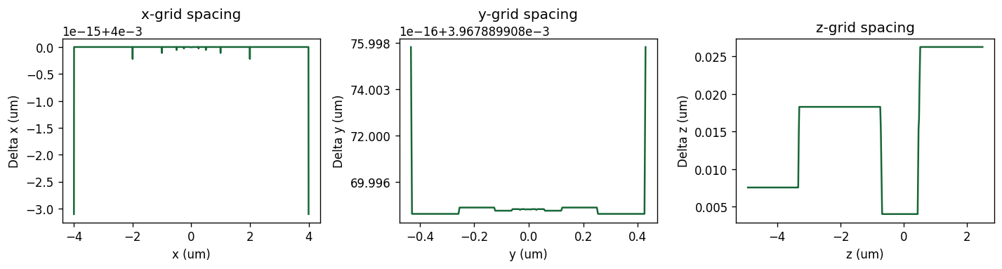
Periodic boundary conditions are applied along $x$ and $y$, while perfectly matched layers terminate the domain along $z$. Mirror symmetries reduce the computational domain for the normally incident, $x$-polarized excitation.
The automatic grid uses at least 60 steps per wavelength. A 4 nm mesh override resolves the BTO, TiO$_2$, and gold region, while a 20 nm override resolves the thick SiO$_2$ layer. These convergence-tested settings match those reported for the supercell simulation in the paper. Because of the fine mesh and long decay time of the high-$Q$ resonance, each cloud simulation may require several hours to complete.
fine_padding = 300 * nm
fine_mesh = td.MeshOverrideStructure(
    geometry=td.Box(
        center=(
            0,
            0,
            0.5 * (max(pillar_height, electrode_height) - bto_thickness) - 100 * nm,
        ),
        size=(
            td.inf,
            td.inf,
            max(pillar_height, electrode_height) + bto_thickness + 2 * fine_padding,
        ),
    ),
    dl=(4 * nm, 4 * nm, 4 * nm),
    enforce=True,
)

oxide_mesh = td.MeshOverrideStructure(
    geometry=td.Box(
        center=(0, 0, -bto_thickness - sio2_thickness / 2),
        size=(td.inf, td.inf, sio2_thickness + 2 * fine_padding),
    ),
    dl=(20 * nm, 20 * nm, 20 * nm),
    shadow=False,
)

grid_spec = td.GridSpec.auto(
    min_steps_per_wvl=60,
    wavelength=design_wavelength,
    override_structures=[fine_mesh, oxide_mesh],
)

boundary_spec = td.BoundarySpec(
    x=td.Boundary.periodic(),
    y=td.Boundary.periodic(),
    z=td.Boundary.pml(),
)

run_time = 50e-12
symmetry = (-1, 1, 0)


def make_spectral_simulation(voltage):
    return td.Simulation(
        center=simulation_center,
        size=simulation_size,
        grid_spec=grid_spec,
        structures=build_structures(voltage),
        sources=[source],
        monitors=[transmission_monitor, resonance_probe],
        boundary_spec=boundary_spec,
        symmetry=symmetry,
        run_time=run_time,
        shutoff=1e-7,
    )


spectral_simulations = {
    f"{voltage:.0f}V": make_spectral_simulation(voltage) for voltage in voltages
}
Sanity checks before submission
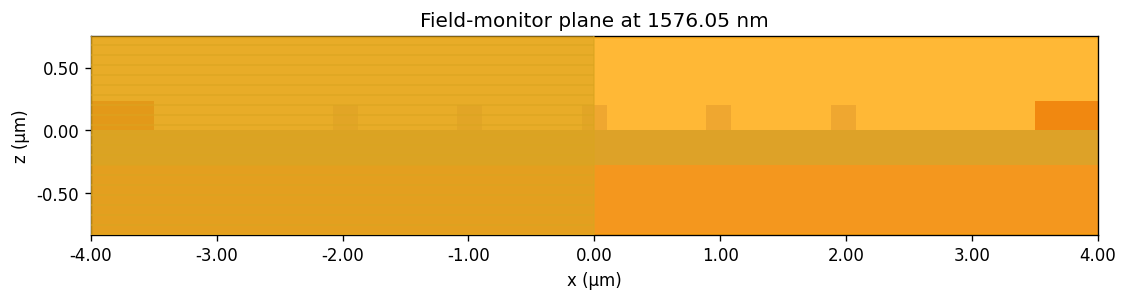
Before submitting the simulations, inspect two representative cross-sections. The first should show five centered TiO$_2$ pillars between the periodic gold electrodes. The second shows the top view through the pillars and verifies the in-plane layout. These checks help identify placement, sign, and layer-stack errors before cloud resources are used.
simulation_0v = spectral_simulations["0V"]

fig, (ax1, ax2) = plt.subplots(1, 2, figsize=(12, 4.2), tight_layout=True)
simulation_0v.plot(y=0, ax=ax1)
ax1.set_title("Device cross-section at y = 0")
ax1.set_xlim(-supercell_x / 2, supercell_x / 2)
ax1.set_ylim(-0.8, 0.8)

simulation_0v.plot(z=pillar_height / 2, ax=ax2)
ax2.set_title("Top view through the TiO2 pillars")
plt.show()

# Check local grid spacing along all three directions.
grid = simulation_0v.grid
fig, axes = plt.subplots(1, 3, figsize=(12, 3.3), tight_layout=True)

for axis, boundaries, coordinate in zip(
    axes,
    (grid.boundaries.x, grid.boundaries.y, grid.boundaries.z),
    ("x", "y", "z"),
):
    boundaries = np.asarray(boundaries)
    axis.plot(boundaries[:-1], np.diff(boundaries))
    axis.set(xlabel=f"{coordinate} (um)", ylabel=f"Delta {coordinate} (um)")
    axis.set_title(f"{coordinate}-grid spacing")

print(
    f"Full simulation grid: "
    f"{simulation_0v.num_cells / 1e6:.2f} million cells"
)

print(
    f"Computational grid after symmetry: "
    f"{simulation_0v.num_computational_grid_points / 1e6:.2f} million cells"
)

plt.show()
Full simulation grid: 315.23 million cells
Computational grid after symmetry: 80.64 million cells
Run the 0, 50, and 100 V spectral simulations
The three complete-device simulations are submitted together as one batch. Before the
solver starts, estimate_cost() reports an upper bound on the required FlexCredits. The
results are downloaded to data/spectra, allowing subsequent notebook sessions to reuse
the local files.
data_directory = Path("data")
data_directory.mkdir(exist_ok=True)

spectral_batch = web.Batch(
    simulations=spectral_simulations,
    folder_name="BTO voltage sweep tutorial",
    verbose=True,
)

estimated_cost = spectral_batch.estimate_cost()
print(f"Estimated maximum batch cost: {estimated_cost:.3f} FlexCredits")

spectral_data = spectral_batch.run(path_dir=data_directory / "spectra")
19:15:00 EDT WARNING: Simulation has 6.57e+06 time steps. The 'run_time' may be
             unnecessarily large, unless there are very long-lived resonances.
19:15:03 EDT WARNING: Simulation has 6.57e+06 time steps. The 'run_time' may be
             unnecessarily large, unless there are very long-lived resonances.
19:15:06 EDT WARNING: Simulation has 6.57e+06 time steps. The 'run_time' may be
             unnecessarily large, unless there are very long-lived resonances.
19:15:09 EDT Maximum FlexCredit cost: 306.732 for the whole batch.
Output()
Estimated maximum batch cost: 306.732 FlexCredits
Started working on Batch containing 3 tasks.
19:15:13 EDT Maximum FlexCredit cost: 306.732 for the whole batch.
             Use 'Batch.real_cost()' to get the billed FlexCredit cost after
             completion.
Output()
19:15:15 EDT Batch complete.
Voltage-dependent transmission
The flux monitor is normalized by the incident source spectrum. Because the wave propagates along $-z$, the signed monitor flux is negated to obtain a positive transmitted-power fraction. The resulting curves show the absolute simulated transmission of the complete device, consistent with the simulated comparison in the paper.
transmission = {}

fig, ax = plt.subplots(figsize=(7.2, 4.4), tight_layout=True)
colors = {0.0: "#355C9A", 50.0: "#D27D2D", 100.0: "#7B4FA3"}

for voltage in voltages:
    task_name = f"{voltage:.0f}V"
    flux_data = spectral_data[task_name]["transmission"].flux
    curve_wavelength_nm = td.C_0 / np.asarray(flux_data.f) / nm
    curve_transmission = -np.real(np.asarray(flux_data))
    order = np.argsort(curve_wavelength_nm)
    transmission[voltage] = {
        "wavelength_nm": curve_wavelength_nm[order],
        "value": curve_transmission[order],
    }
    ax.plot(
        transmission[voltage]["wavelength_nm"],
        transmission[voltage]["value"],
        lw=1.8,
        color=colors[voltage],
        label=f"{voltage:.0f} V",
    )

ax.set(
    xlabel="Wavelength (nm)",
    ylabel="Transmission",
    title="Hybrid BTO/TiO2 metasurface",
    xlim=(wavelength_nm.min(), wavelength_nm.max()),
)
ax.legend(frameon=False)
ax.grid(alpha=0.2)
plt.show()
Automatically select the strongest resonant field
For a Fano resonance, a transmission extremum does not necessarily coincide exactly with the wavelength of maximum internal field enhancement. The resonant-field wavelength is therefore selected from the 0 V line monitor by maximizing
$$I_{\mathrm{probe}}(\lambda) = \left\langle |E_x(x,y=0,z=-t_{\mathrm{BTO}}/2;\lambda)|^2\right\rangle_x.$$
This procedure identifies the field maximum directly while keeping the broadband monitor data compact.
probe_ex = spectral_data["0V"]["resonance_probe"].Ex.squeeze(drop=True)
spatial_dimensions = [dimension for dimension in probe_ex.dims if dimension != "f"]
probe_intensity = (np.abs(probe_ex) ** 2).mean(dim=spatial_dimensions)

probe_frequencies = np.asarray(probe_intensity.f)
probe_wavelength_nm = td.C_0 / probe_frequencies / nm
probe_values = np.asarray(probe_intensity)

strongest_index = int(np.nanargmax(probe_values))
resonance_frequency = float(probe_frequencies[strongest_index])
resonance_wavelength = td.C_0 / resonance_frequency

order = np.argsort(probe_wavelength_nm)
fig, ax = plt.subplots(figsize=(7.2, 4.0), tight_layout=True)
ax.plot(probe_wavelength_nm[order], probe_values[order], color="#B04A5A")
ax.axvline(resonance_wavelength / nm, color="0.2", ls="--", lw=1)
ax.set(
    xlabel="Wavelength (nm)",
    ylabel=r"Mean $|E_x|^2$ in the BTO probe line (a.u.)",
    title=f"Strongest field at {resonance_wavelength / nm:.2f} nm",
)
ax.grid(alpha=0.2)
plt.show()

print(f"Selected resonance wavelength: {resonance_wavelength / nm:.3f} nm")
print(f"Selected resonance frequency: {resonance_frequency / 1e12:.3f} THz")
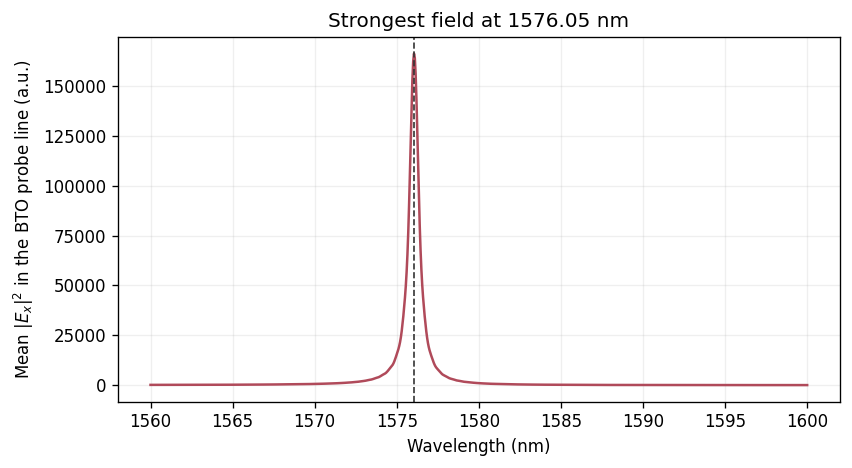
Selected resonance wavelength: 1576.050 nm
Selected resonance frequency: 190.218 THz
Resonant field simulation
Once the resonant-field wavelength has been identified, a single-frequency simulation is performed at that wavelength. Two field monitors and one permittivity monitor are used:
-
field_xzrecords $E_x$ in the $x$-$z$ plane through the nanopillar centers, matching the cross-section shown in Fig. 1d. -
field_volumerecords all three electric-field components within a 2.4 µm-high volume spanning the periodic supercell. -
epsilon_volumerecords the relative permittivity on the corresponding volume.
The 2.4 µm vertical span encloses the resonant near field around the metasurface. It can be increased if a convergence test with respect to the vertical integration window is desired.
field_z_min = -bto_thickness - 0.55 * um
field_z_max = pillar_height + 0.55 * um
field_plane_center_z = 0.5 * (field_z_min + field_z_max)
field_plane_span_z = field_z_max - field_z_min

field_plane_monitor = td.FieldMonitor(
    center=(0, 0, field_plane_center_z),
    size=(td.inf, 0, field_plane_span_z),
    freqs=[resonance_frequency],
    fields=["Ex"],
    interval_space=(2, 1, 2),
    colocate=True,
    name="field_xz",
)

confinement_volume_center = (0, 0, 0)
confinement_volume_size = (td.inf, td.inf, 2.4 * um)

field_volume_monitor = td.FieldMonitor(
    center=confinement_volume_center,
    size=confinement_volume_size,
    freqs=[resonance_frequency],
    fields=["Ex", "Ey", "Ez"],
    interval_space=(2, 1, 2),
    colocate=True,
    name="field_volume",
)

epsilon_volume_monitor = td.PermittivityMonitor(
    center=confinement_volume_center,
    size=confinement_volume_size,
    freqs=[resonance_frequency],
    interval_space=(2, 1, 2),
    name="epsilon_volume",
)

resonant_source = source.updated_copy(
    source_time=td.GaussianPulse(
        freq0=resonance_frequency,
        fwidth=resonance_frequency / 20,
    )
)

field_simulation = spectral_simulations["0V"].updated_copy(
    sources=[resonant_source],
    monitors=[field_plane_monitor, field_volume_monitor, epsilon_volume_monitor],
)

fig, ax = plt.subplots(figsize=(9.5, 3.0), tight_layout=True)
field_simulation.plot(y=0, ax=ax)
ax.set(xlim=(-supercell_x / 2, supercell_x / 2), ylim=(field_z_min, field_z_max))
ax.set_title(f"Field-monitor plane at {resonance_wavelength / nm:.2f} nm")
plt.show()
field_job = web.Job(
    simulation=field_simulation,
    task_name="BTO 0V resonant field and confinement",
    verbose=True,
)

estimated_field_cost = field_job.estimate_cost()
print(f"Estimated maximum field-run cost: {estimated_field_cost:.3f} FlexCredits")

field_data = field_job.run(path=data_directory / "BTO_0V_resonant_field.hdf5")
19:15:16 EDT WARNING: Simulation has 6.57e+06 time steps. The 'run_time' may be
             unnecessarily large, unless there are very long-lived resonances.
             Created task 'BTO 0V resonant field and confinement' with
             resource_id 'fdve-7d40ad0e-ba9b-4508-a53d-44adae7590af' and
             task_type 'FDTD'.
             View task using web UI at
             'https://tidy3d.simulation.cloud/workbench?taskId=fdve-7d40ad0e-ba9
             b-4508-a53d-44adae7590af'.
Task folder: 'default'.
Output()
19:15:19 EDT Estimated FlexCredit cost: 101.754. This assumes the FDTD solver
             runs for the full simulation time; if early shutoff is reached, the
             billed cost can be lower. Use 'web.real_cost(task_id)' to get the
             billed FlexCredit cost after a simulation run.
Estimated maximum field-run cost: 101.754 FlexCredits
19:15:20 EDT status = success
Output()
19:15:30 EDT Loading results from data/BTO_0V_resonant_field.hdf5
$x$-$z$ field profile through the nanopillar centers
The plot shows $|E_x|$ in arbitrary units. The dashed rectangle marks the BTO active region used in the numerator of the confinement factor: the portion of the BTO layer beneath the five metasurface unit cells. The plotted plane and active-region definition correspond to those used in Fig. 1d.
fig, ax = plt.subplots(figsize=(10.5, 3.4), tight_layout=True)
field_data.plot_field(
    field_monitor_name="field_xz",
    field_name="Ex",
    val="abs",
    eps_alpha=0.22,
    ax=ax,
)

active_outline = Rectangle(
    (-active_region_width / 2, -bto_thickness),
    active_region_width,
    bto_thickness,
    fill=False,
    edgecolor="white",
    linewidth=1.2,
    linestyle="--",
    label="BTO active region",
)
ax.add_patch(active_outline)
ax.set(
    xlim=(-supercell_x / 2, supercell_x / 2),
    ylim=(field_z_min, field_z_max),
    xlabel="x (um)",
    ylabel="z (um)",
    title=rf"$|E_x|$ at {resonance_wavelength / nm:.2f} nm",
)
ax.legend(loc="upper right", frameon=True)
plt.show()
Optical confinement factor
Following the definition in the paper, the active-region optical confinement factor is
$$\Gamma_{\mathrm{AR}}= \frac{\iiint_{\mathrm{AR}}\varepsilon_{\mathrm{BTO}}|E_x|^2\,dV} {\iiint_{\mathrm{SC}}\varepsilon(\mathbf r)|\mathbf E|^2\,dV}.$$
The active region is the BTO volume beneath the five TiO$_2$ unit cells: $|x|\le 2.475\ \mathrm{\mu m}$, the full periodic $y$ span, and $-t_{\mathrm{BTO}}\le z\le0$. The denominator is integrated over the monitored supercell volume. All electric-field components are colocated before integration, and the directional permittivity samples are interpolated onto the corresponding field coordinates. The common electric-energy prefactor cancels in the ratio.
At telecommunication wavelengths, the real part of the gold permittivity is negative, so the $\operatorname{Re}(\varepsilon)|E|^2$ weighting is not positive definite inside the metal. The primary value reported below follows the definition above. As a sensitivity check, a second value is calculated after setting contributions from negative-permittivity grid points to zero. Comparing the two values quantifies whether the gold region has a meaningful influence on the extracted confinement factor; it does not redefine $\Gamma_{\mathrm{AR}}$.
import gc

field_volume = field_data["field_volume"]
epsilon_volume = field_data["epsilon_volume"]


def component_integrals(field, epsilon, active=False):
    """Calculate one field component at a time to limit memory usage."""

    # Interpolate the permittivity onto the corresponding field grid.
    epsilon = epsilon.interp_like(field, method="linear")
    re_epsilon = np.real(epsilon)

    # Electric-field weighting used in the confinement-factor definition.
    density = re_epsilon * np.abs(field) ** 2

    total = density.integrate(coord=("x", "y", "z")).item()

    # Sensitivity check: exclude the negative-permittivity Au region.
    positive_density = density.where(re_epsilon > 0, other=0)
    total_positive = positive_density.integrate(
        coord=("x", "y", "z")
    ).item()

    # Only the x-polarized field in the BTO active region enters the numerator.
    active_energy = 0
    if active:
        active_density = density.sel(
            x=slice(
                -active_region_width / 2,
                active_region_width / 2,
            ),
            z=slice(-bto_thickness, 0),
        )
        active_energy = active_density.integrate(
            coord=("x", "y", "z")
        ).item()

    # Release intermediate 3D arrays before processing the next component.
    del epsilon, re_epsilon, density, positive_density
    gc.collect()

    return (
        float(np.real(total)),
        float(np.real(total_positive)),
        float(np.real(active_energy)),
    )


energy_supercell = 0
energy_excluding_negative_eps = 0
energy_active_region = 0

# Process Ex, Ey, and Ez sequentially to reduce peak memory use.
for field_name, epsilon_name in (
    ("Ex", "eps_xx"),
    ("Ey", "eps_yy"),
    ("Ez", "eps_zz"),
):
    field = getattr(field_volume, field_name).isel(f=0, drop=True)
    epsilon = getattr(epsilon_volume, epsilon_name).isel(f=0, drop=True)

    total, positive, active = component_integrals(
        field,
        epsilon,
        active=(field_name == "Ex"),
    )

    energy_supercell += total
    energy_excluding_negative_eps += positive
    energy_active_region += active

    del field, epsilon
    gc.collect()


# Primary result following the confinement-factor definition.
confinement_factor = energy_active_region / energy_supercell

# Secondary result used only to assess the influence of the Au region.
confinement_without_au = (
    energy_active_region
    / energy_excluding_negative_eps
)

relative_change = confinement_without_au / confinement_factor - 1

print(f"Gamma_AR: {confinement_factor:.4f}")
print(
    "Gamma_AR without the negative-permittivity region: "
    f"{confinement_without_au:.4f}"
)
print(f"Relative change: {relative_change:.3%}")
Gamma_AR: 0.7890
Gamma_AR without the negative-permittivity region: 0.7882
Relative change: -0.113%
The calculated confinement factor is consistent with the value of $\sim 0.8$ reported in the paper. This confirms that the resonant optical field is strongly confined to the $x$-polarized component within the BTO active region.



 TERMS & CONDITIONS


 How the process works:
 Try this real URL to see an example: