





Joshua Mornhinweg, Harvard John A. Paulson School of Engineering and Applied Sciences
Cavity quantum electrodynamics enters the deep-strong coupling regime when the vacuum Rabi frequency $\Omega_\mathrm{R}$ of a light-matter system becomes comparable to, or larger than, the bare transition frequency $\omega_\mathrm{c}$ of the matter excitation. Reaching $\Omega_\mathrm{R}/\omega_\mathrm{c} \gtrsim 1$ requires squeezing the electromagnetic vacuum field into a mode volume far below $(\lambda/2)^3$, because the single-photon field amplitude scales as $E_\mathrm{vac} \propto 1/\sqrt{V}$.
In the terahertz (THz) range this is often done with a planar metallic metasurface evaporated directly onto a substrate. The metasurface acts as an array of sub-wavelength LC resonators that concentrate the THz vacuum field into the near-field volume just below the metal, where it overlaps with our matter system of choice.
This notebook reproduces the bare THz resonator of
J. Mornhinweg, L. K. Diebel, M. Halbhuber, M. Prager, J. Riepl, T. Inzenhofer, D. Bougeard, R. Huber, and C. Lange, Mode-multiplexing deep-strong light-matter coupling, Nature Communications 15, 1847 (2024).
The bare resonator that we can compute here supports several well-separated modes - a fundamental LC resonance at $\nu_1 \approx 0.5$ THz and a higher-order mode at $\nu_2 \approx 2$ THz - which couple simultaneously to a comb of magnetoplasmon modes. In particular, this resonator geometry features an extremely compact unit cell. Rather than isolating individual resonators, the design uses an inverted (complementary, Babinet-type) layout in which the metal is continuous and the aperture is patterned. Regions of low current density are removed and adjacent current paths of opposite phase are merged, shrinking the unit cell from a conventional 60 x 60 μm to only 30 x 32.5 μm.
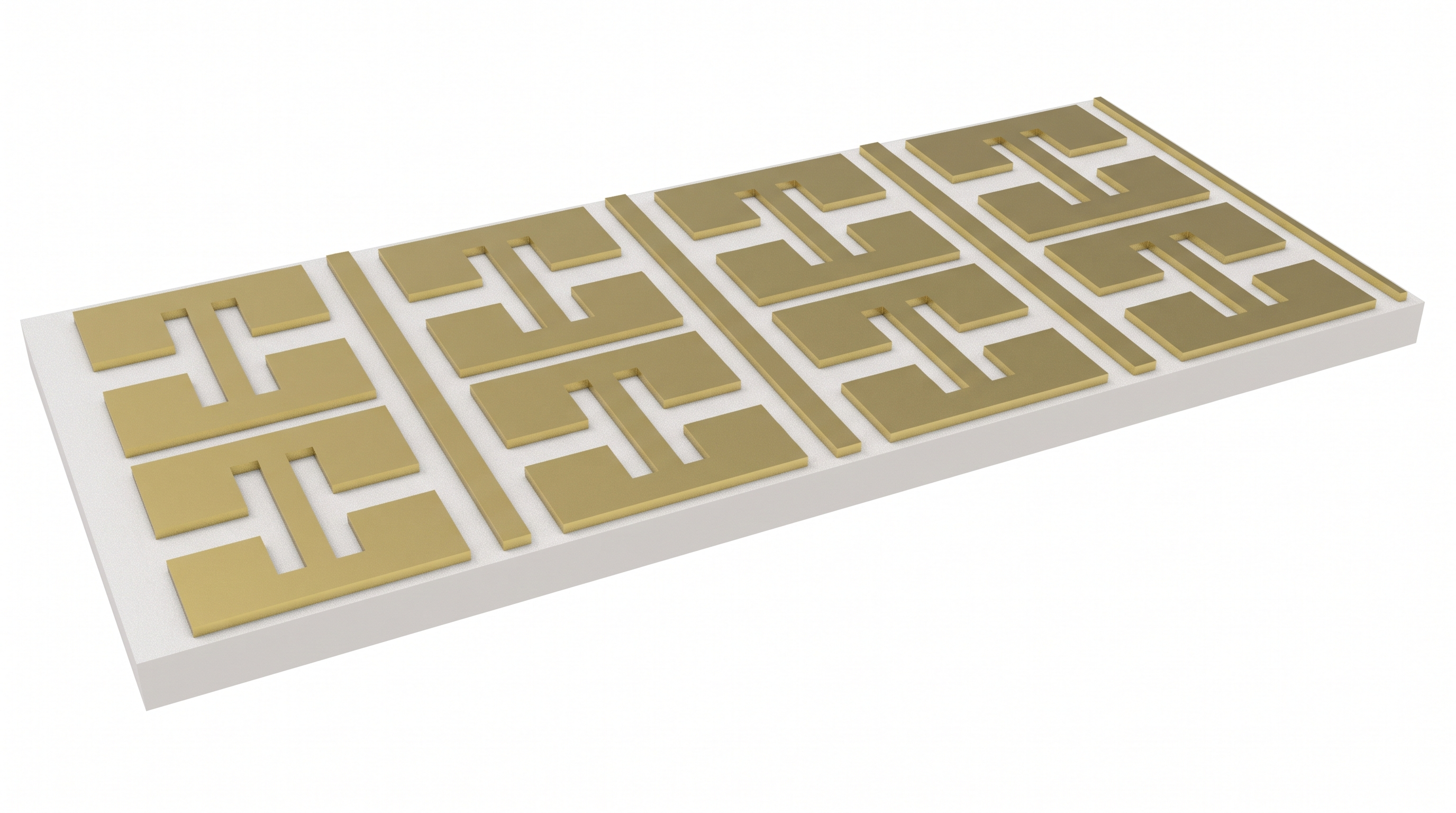
**Note: Resonances will differ slightly between versions. The presented notebook was run on Tidy3D 2.9.3
What this notebook computes
We model a single unit cell of the metasurface with periodic boundaries, illuminated by a normally incident, broadband THz plane wave, and extract
- the transmittance, reflectance and absorptance spectra from 0.1 to 6 THz, from which the resonator mode frequencies are read off, and
- the electric near-field distributions of the first two modes just below the metal - the quantity that determines the coupling strength to the matter system.
Model simplifications. As in the near-field analysis of the paper, we simulate the bare resonator on an undoped substrate: there are no quantum wells, no two-dimensional electron gas and no external magnetic field, so no polariton splitting appears here. GaAs is treated as a lossless, dispersionless dielectric with $\varepsilon = 12.9$, which is accurate across the THz band. The gold film is 200 nm thick and is described by a surface-impedance model at the literature conductivity of gold. Finally, the array is taken to be infinite and the illumination to be a plane wave, whereas the experiment uses a finite array and a focused THz beam.
import matplotlib.pyplot as plt
import numpy as np

import tidy3d as td
import tidy3d.web as web
Simulation setup
Frequency range
The resonator modes of interest lie between roughly 0.5 and 2 THz, but the metasurface is designed to couple to a magnetoplasmon comb spanning several octaves, so we record the spectra over the full 0.1-6 THz window. All lengths in Tidy3D are in micrometers and all frequencies in Hz.
THz = 1e12  # conversion factor from THz to Hz

f_min = 0.1 * THz  # lower edge of the band of interest
f_max = 6.0 * THz  # upper edge of the band of interest

freqs = np.linspace(f_min, f_max, 300)  # frequencies recorded by the monitors
freq0 = 0.5 * (f_min + f_max)  # central frequency of the source pulse
fwidth = freq0 / 2  # spectral width of the source pulse

lda0 = td.C_0 / freq0  # central wavelength in vacuum (um)
lda_max = td.C_0 / f_min  # longest wavelength in vacuum (um)

print(f"central frequency  : {freq0 / THz:.2f} THz  (lambda0 = {lda0:.1f} um)")
print(f"longest wavelength : {lda_max:.0f} um in vacuum")
central frequency  : 3.05 THz  (lambda0 = 98.3 um)
longest wavelength : 2998 um in vacuum
Materials
Two materials are involved. The substrate is semi-insulating GaAs, which is essentially transparent and dispersion-free below the reststrahlen band, so a constant relative permittivity $\varepsilon = 12.9$ is an excellent approximation throughout the THz range.
The metasurface is gold, and here the choice of model matters more than it might seem. A Drude metal at THz frequencies has an enormous permittivity - $|\varepsilon| \sim 10^6$, i.e. a refractive index above 2000 - so the wavelength inside the gold is only a fraction of a micron. An automatic mesher will faithfully try to resolve that, and the grid explodes: the volumetric Drude version of this simulation needs a near-uniform 0.1 um grid and roughly $7 \times 10^6$ cells, almost all of them spent inside a metal whose interior carries no useful physics.
The physics of such a large $|\varepsilon|$ is simply that the field penetrates one skin
depth and stops. That is what a surface impedance boundary condition (SIBC) encodes, and
is implemented in LossyMetalMedium: the metal volume is replaced by a surface impedance $Z_s = \sqrt{i \mu_0 \omega / \sigma}$
applied at its boundary, so the mesh never has to enter the gold.
Three things to note about the arguments:
-
conductivityis in S/um, not S/m. Literature gold has $\sigma = 4.1 \times 10^7$ S/m, hence41.0. -
frequency_rangeis required - the impedance is fitted with a pole-residue model over that band, and construction raises a validation error without it. -
thicknessswitches on a one-dimensional transmission-line correction for a film that is not many skin depths thick. At 200 nm and $\delta \approx 100$ nm it is a small effect (it changes $Z_s$ by about 3% at 0.57 THz and under 1% at 2.15 THz), but it is the physically correct model for a film this thin.
SIBC is accurate when the skin depth is much smaller than the feature size. Here $\delta \approx 100$ nm against 2.5 um slots - a factor of 25 - so we are comfortably inside its range of validity.
eps_GaAs = 12.9  # relative permittivity of GaAs in the THz range
GaAs = td.Medium(permittivity=eps_GaAs)

# --- layer stack -----------------------------------------------------------
t_metal = 0.2  # gold film thickness (um)
t_GaAs = 5000.0  # GaAs substrate thickness (um) - extends through the PML

# --- gold, as a surface-impedance conductor --------------------------------
sigma_Au = 41.0  # S/um  (= 4.1e7 S/m, the literature DC conductivity of gold)

gold = td.LossyMetalMedium(
    conductivity=sigma_Au,
    frequency_range=(f_min, f_max),  # required: the impedance model is fitted over this band
    thickness=t_metal,  # thin-film transmission-line correction for the 200 nm layer
)

vacuum = td.Medium()  # background medium above the metasurface
Unit-cell geometry
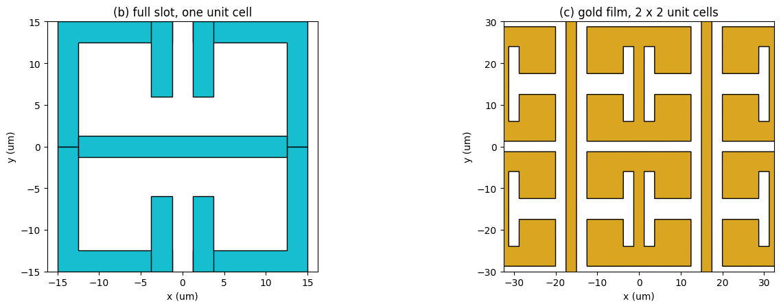
The metasurface is an inverted structure: a continuous gold film perforated by a butterfly-shaped aperture. It is easiest to construct the aperture first and then subtract it from an unbroken film, which is exactly how the design is conceived - the complementary counterpart of four LC resonators sharing their inductive loops.
The aperture has the full symmetry of the unit cell about both mirror planes, which can later also be used to reduce the simulation load.
# --- unit cell -------------------------------------------------------------
period_x = 32.5  # unit-cell period along x (um)
period_y = 30.0  # unit-cell period along y (um)

# --- aperture pattern ------------------------------------------------------
ap_x = 30.0  # total extent of the aperture pattern along x (um)
ap_y = 30.0  # total extent of the aperture pattern along y (um)
w_gap = 2.5  # width of the central capacitive gap (um)
w_bar = 2.5  # width of the slots forming the inductive loop (um)
l_cap = 9.0  # length of the capacitor arm (um)
def slot(x0, x1, y0, y1):
    """Axis-aligned box spanning [x0, x1] x [y0, y1], extruded over the metal thickness."""
    return td.Box.from_bounds(rmin=(x0, y0, 0), rmax=(x1, y1, t_metal))


# quarter of the aperture, in the first quadrant
outer = slot(w_gap / 2, ap_x / 2, 0, ap_y / 2)
inner = slot(0, ap_x / 2 - w_bar, 0, ap_y / 2 - w_bar)
arm = slot(w_gap / 2, w_gap / 2 + w_bar, ap_y / 2 - l_cap, ap_y / 2)

quarter = (outer - inner) + arm

# mirror the quarter into the remaining three quadrants
mirror_x = td.Transformed(geometry=quarter, transform=td.Transformed.scaling(x=-1))
mirror_y = td.Transformed(geometry=quarter, transform=td.Transformed.scaling(y=-1))
mirror_xy = td.Transformed(geometry=mirror_x, transform=td.Transformed.scaling(y=-1))

# horizontal slot bridging the two halves through the centre of the cell
bridge = slot(-(ap_x / 2 - w_bar), ap_x / 2 - w_bar, -w_bar / 2, w_bar / 2)

aperture = quarter + mirror_x + mirror_y + mirror_xy + bridge

# the metasurface is the complement of the aperture in a continuous gold film
metal_film = td.Box(center=(0, 0, t_metal / 2), size=(td.inf, td.inf, t_metal))

metasurface = td.Structure(
    geometry=metal_film - aperture,
    medium=gold,
    name="metasurface",
)

substrate = td.Structure(
    geometry=td.Box(center=(0, 0, -t_GaAs / 2), size=(td.inf, td.inf, t_GaAs)),
    medium=GaAs,
    name="substrate",
)
# tile the aperture over neighbouring cells, for visualization only
tiles = [
    td.Transformed(
        geometry=aperture,
        transform=td.Transformed.translation(x=i * period_x, y=j * period_y, z=0),
    )
    for i in (-1, 0, 1)
    for j in (-1, 0, 1)
]
gold_tiled = metal_film - td.GeometryGroup(geometries=tiles)

fig, axes = plt.subplots(1, 2, figsize=(14, 4.6), tight_layout=True)


aperture.plot(z=t_metal / 2, ax=axes[0], facecolor="tab:cyan", edgecolor="k")
axes[0].set_title("(b) full slot, one unit cell")
axes[0].set_xlim(-period_x / 2, period_x / 2)
axes[0].set_ylim(-period_y / 2, period_y / 2)

gold_tiled.plot(z=t_metal / 2, ax=axes[1], facecolor="goldenrod", edgecolor="k")
axes[1].set_title("(c) gold film, 2 x 2 unit cells")
axes[1].set_xlim(-period_x, period_x)
axes[1].set_ylim(-period_y, period_y)

for ax in axes:
    ax.set_aspect("equal")
    ax.set_xlabel("x (um)")
    ax.set_ylabel("y (um)")
plt.show()
Source and monitors
The metasurface is excited from above by a broadband plane wave at normal incidence. The capacitive
gap runs along $x$, so the mode is driven by a field polarized along $y$; we set pol_angle to
$90^\circ$ accordingly.
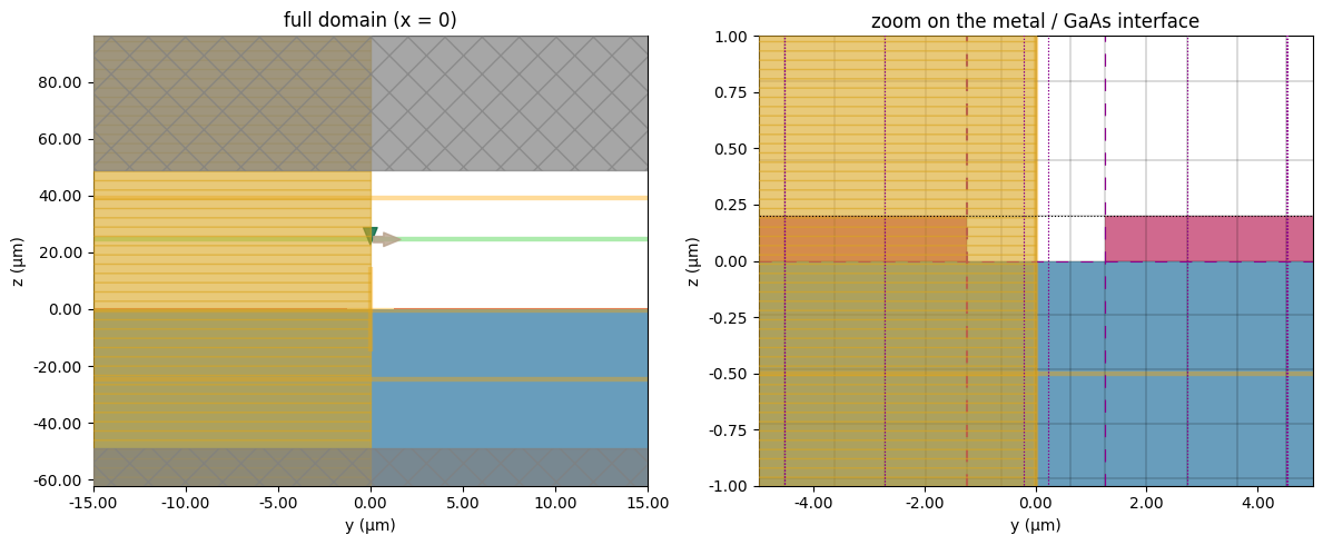
Along $z$ the domain is one central wavelength high, with the GaAs filling the lower half and extending through the PML so that the substrate is effectively semi-infinite and no back-surface echo appears in the spectrum.
Four monitors record the response:
-
T- a flux monitor inside the GaAs, below the metasurface, giving the transmittance, -
R- a flux monitor above the source, giving the reflectance (a plane-wave source radiates in one direction only, so everything crossing this plane is reflected light), -
field_xy- the in-plane electric field 0.5 um below the metal, i.e. at the example depth of the matter system, at the two resonance frequencies, -
field_xz- a vertical cut through the cell showing how far the near field reaches into the substrate.
offset = lda0 / 4  # spacing between the domain edge and the source / monitor planes
Lz = 4 * offset  # height of the simulation domain (= lda0)

# frequencies at which the near fields are recorded: the two resonator modes.
f_modes = np.array([0.55, 2.11]) * THz

source = td.PlaneWave(
    name="plane_wave",
    center=(0, 0, Lz / 2 - offset),
    size=(td.inf, td.inf, 0),
    source_time=td.GaussianPulse(freq0=freq0, fwidth=fwidth),
    direction="-",
    pol_angle=np.pi / 2,  # E field along y, across the capacitive gap
)

monitor_t = td.FluxMonitor(
    name="T",
    center=(0, 0, -Lz / 2 + offset),
    size=(td.inf, td.inf, 0),
    freqs=freqs,
    normal_dir="-",  # power flowing downwards counts as positive
)

monitor_r = td.FluxMonitor(
    name="R",
    center=(0, 0, 0.4 * Lz),
    size=(td.inf, td.inf, 0),
    freqs=freqs,
    normal_dir="+",  # power flowing upwards counts as positive
)

monitor_field_xy = td.FieldMonitor(
    name="field_xy",
    center=(0, 0, -0.5),
    size=(td.inf, td.inf, 0),
    freqs=f_modes,
)

monitor_field_xz = td.FieldMonitor(
    name="field_xz",
    center=(0, 0, 0),
    size=(td.inf, 0, 30),
    freqs=f_modes,
)
Boundaries, mesh and symmetry
The array is periodic in $x$ and $y$ and absorbing in $z$. Because the excitation is a normally incident plane wave, simple periodic boundaries are sufficient - Bloch boundaries would only be needed at oblique incidence.
With the metal reduced to a surface impedance, the mesh is driven entirely by the dielectric problem. We define dl_min as a guard rail against runaway refinement. Here we have two places where resolution is required:
-
In plane, the narrow features are the 2.5 μm slots and bars.
min_steps_per_wvl = 25plus a corner refinement gives roughly 0.5 μm cells. -
In $z$, the near field below the metal is what couples to our matter excitation. It decays over a
few microns. Left to itself
AutoGridputs ~2.6 μm cells at the surface, which would smear that decay into a single cell and make the near-field maps meaningless. AMeshOverrideStructurepins the step todz_nearthrough the topz_nearmicrons of the substrate.
Finally, with $\mathbf{E} \parallel \hat{y}$ the field has a definite parity about both mirror
planes: $E_y$ is even under $x \to -x$ and odd under $y \to -y$, giving symmetry=(1, -1, 0). This
cuts the computational domain - and therefore the cost - by a factor of four.
# --- meshing ---------------------------------------------------------------
dl_min = 0.2  # smallest allowed grid step (um)
min_steps_per_wvl = 25  # base resolution
dz_near = 0.25  # z step in the near-field region below the metal (um)
z_near = 6.0  # depth of that refined region (um)


boundary_spec = td.BoundarySpec(
    x=td.Boundary.periodic(),
    y=td.Boundary.periodic(),
    z=td.Boundary.pml(),
)

grid_spec = td.GridSpec(
    grid_x=td.AutoGrid(dl_min=dl_min, min_steps_per_wvl=min_steps_per_wvl),
    grid_y=td.AutoGrid(dl_min=dl_min, min_steps_per_wvl=min_steps_per_wvl),
    grid_z=td.AutoGrid(dl_min=dl_min, min_steps_per_wvl=min_steps_per_wvl),
)

# refine around the in-plane corners of the aperture, where the fields are singular
corner_spec = td.LayerRefinementSpec.from_structures(
    axis=2,
    structures=[metasurface],
    corner_refinement=td.GridRefinement(refinement_factor=4),
)

# resolve the near field in the top few microns of the substrate, where the
# quantum wells would sit; AutoGrid on its own would put ~2.6 um cells here
near_field_mesh = td.MeshOverrideStructure(
    geometry=td.Box.from_bounds(
        rmin=(-td.inf, -td.inf, -(z_near - t_metal)),
        rmax=(td.inf, td.inf, t_metal),
    ),
    dl=(None, None, dz_near),
)

grid_spec = grid_spec.updated_copy(
    layer_refinement_specs=[corner_spec],
    override_structures=[near_field_mesh],
)
run_time = 2e-10

sim = td.Simulation(
    size=(period_x, period_y, Lz),
    grid_spec=grid_spec,
    structures=[substrate, metasurface],
    sources=[source],
    monitors=[monitor_t, monitor_r, monitor_field_xy, monitor_field_xz],
    run_time=run_time,
    medium=vacuum,
    boundary_spec=boundary_spec,
    symmetry=(1, -1, 0),
    shutoff=1e-8,
)

dl = [np.diff(np.array(b)) for b in sim.grid.boundaries.to_list]
print(f"grid cells : {np.prod(sim.grid.num_cells):.2e}")
print(f"time steps : {sim.num_time_steps:.2e}")
print(f"min step   : dx={dl[0].min():.3f}  dy={dl[1].min():.3f}  dz={dl[2].min():.3f} um")

# for reference, the volumetric-Drude version of this same simulation needs
# 6.75e6 cells and 1.05e6 time steps - about 70x more work.
16:01:21 EDT WARNING: Structure: 'metasurface' (simulation.structures[1]) was
             detected as being less than half of a central wavelength from a PML
             on side z-max. To avoid inaccurate results or divergence, please
             increase gap between any structures and PML or fully extend
             structure through the pml.
             WARNING:  ℹ️ ⚠️ RF simulations are subject to new license
             requirements in the future. You are using RF-specific components in
             this simulation.
              - Contains a 'LossyMetalMedium'.
              - Contains monitors defined for RF wavelengths.
grid cells : 2.76e+05
time steps : 3.49e+05
min step   : dx=0.491  dy=0.494  dz=0.200 um
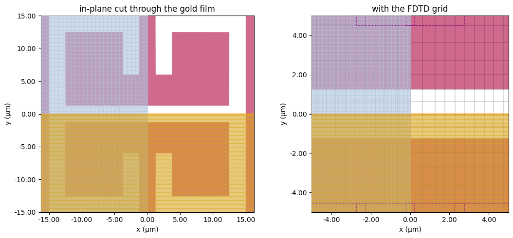
Sanity checks before submitting
fig, (ax1, ax2) = plt.subplots(1, 2, figsize=(11, 5), tight_layout=True)

sim.plot(z=t_metal / 2, ax=ax1)
ax1.set_title("in-plane cut through the gold film")

sim.plot(z=t_metal / 2, ax=ax2)
sim.plot_grid(z=t_metal / 2, ax=ax2)
ax2.set_title("with the FDTD grid")
ax2.set_xlim(-5, 5)
ax2.set_ylim(-5, 5)
plt.show()
fig, (ax1, ax2) = plt.subplots(1, 2, figsize=(12, 5), tight_layout=True)

sim.plot(x=0, ax=ax1)
ax1.set_title("full domain (x = 0)")
ax1.set_aspect("auto")  # the domain is 30 um wide and 98 um tall

sim.plot(x=0, ax=ax2)
sim.plot_grid(x=0, ax=ax2)
ax2.set_title("zoom on the metal / GaAs interface")
ax2.set_xlim(-5, 5)
ax2.set_ylim(-1, 1)
ax2.set_aspect("auto")
plt.show()
Running the simulation
job = web.Job(simulation=sim, task_name="thz_metasurface_resonator", verbose=True)
estimated_cost = job.estimate_cost()
16:01:22 EDT Created task 'thz_metasurface_resonator' with task_id
             'fdve-19b0a112-98ea-4486-b7df-2bacf79cdff3' and task_type 'FDTD'.
             View task using web UI at
             'https://tidy3d.simulation.cloud/workbench?taskId=fdve-19b0a112-98e
             a-4486-b7df-2bacf79cdff3'.
Task folder: 'default'.
Output()
16:01:24 EDT Maximum FlexCredit cost: 0.025. Minimum cost depends on task
             execution details. Use 'web.real_cost(task_id)' to get the billed
             FlexCredit cost after a simulation run.
16:01:25 EDT Maximum FlexCredit cost: 0.025. Minimum cost depends on task
             execution details. Use 'web.real_cost(task_id)' to get the billed
             FlexCredit cost after a simulation run.
sim_data = job.run(path="data/simulation_data.hdf5")
status = success
Output()
16:01:26 EDT loading simulation from data/simulation_data.hdf5
             WARNING: Structure: 'metasurface' (simulation.structures[1]) was
             detected as being less than half of a central wavelength from a PML
             on side z-max. To avoid inaccurate results or divergence, please
             increase gap between any structures and PML or fully extend
             structure through the pml.
             WARNING: Simulation final field decay value of 1.42e-06 is greater
             than the simulation shutoff threshold of 1e-08. Consider running
             the simulation again with a larger 'run_time' duration for more
             accurate results.
             WARNING: Warning messages were found in the solver log. For more
             information, check 'SimulationData.log' or use
             'web.download_log(task_id)'.
Results
Transmittance, reflectance and absorptance
Tidy3D normalizes flux monitors by the power spectrum of the source, so the recorded fluxes are directly the transmittance $T$ and reflectance $R$; the absorptance follows as $A = 1 - R - T$ and, since GaAs is lossless here, it measures ohmic dissipation in the gold alone.
For an aperture (Babinet-complementary) metasurface the resonances appear as transmission peaks rather than dips: on resonance the slot radiates efficiently into the substrate, while off resonance the continuous metal film reflects almost everything.
We also plot $\sqrt{T}$, the field transmission amplitude, since that is the quantity measured directly by THz time-domain spectroscopy, where the transmitted electric field $E(t)$ is sampled electro-optically.
def find_peaks(x, y, height=0.1):
    """Positions and heights of local maxima of y(x) above a threshold."""
    i = np.arange(1, len(y) - 1)
    mask = (y[i] > y[i - 1]) & (y[i] > y[i + 1]) & (y[i] > height)
    return x[i][mask], y[i][mask]


T = sim_data["T"].flux.values
R = sim_data["R"].flux.values
A = 1 - R - T

f_thz = freqs / THz
f_peak, T_peak = find_peaks(f_thz, T, height=0.1)

fig, (ax1, ax2) = plt.subplots(2, 1, figsize=(8, 7), sharex=True, tight_layout=True)

ax1.plot(f_thz, T, label="$T$")
ax1.plot(f_thz, R, label="$R$")
ax1.plot(f_thz, A, label="$A$")
ax1.set_ylabel("normalized power")
ax1.set_ylim(0, 1)
ax1.legend()
ax1.set_title("metasurface response at normal incidence")

ax2.plot(f_thz, np.sqrt(T), color="k")
ax2.plot(f_peak, np.sqrt(T_peak), "v", color="tab:red", ms=8)
for fp, tp in zip(f_peak[:2], T_peak[:2]):
    ax2.annotate(
        f"{fp:.2f} THz",
        xy=(fp, np.sqrt(tp)),
        xytext=(0, 12),
        textcoords="offset points",
        ha="center",
        color="tab:red",
    )
ax2.set_xlabel("frequency (THz)")
ax2.set_ylabel("field transmission $\\sqrt{T}$")
ax2.set_xlim(0, 6)
ax2.set_ylim(0, 1)

plt.show()

print("resonances found at (THz):", np.round(f_peak, 3))
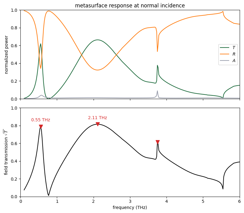
resonances found at (THz): [0.554 2.113 3.751]
The two lowest peaks are the modes that carry the coupling in the experiment; compare them against the measured $\nu_1 = 0.52$ THz and $\nu_2 = 1.95$ THz. Some offset is expected from the idealizations listed at the top - nominal rather than fabricated dimensions.
Near-field distributions of the two modes
The coupling strength is set not by the transmittance but by how tightly the vacuum field is confined where the matter system is located. The map below shows $|\mathbf{E}|$ in a plane 0.5 um below the gold at each of the two resonance frequencies.
fig, axes = plt.subplots(1, 2, figsize=(12, 4.8), tight_layout=True)

for ax, f_i, label in zip(axes, f_modes, ["nu_1", "nu_2"]):
    sim_data.plot_field("field_xy", "E", val="abs", f=f_i, ax=ax)
    ax.set_title(f"{label} = {f_i / THz:.2f} THz")
    ax.set_aspect("equal")

plt.show()
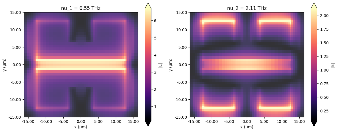
What to look for: an LC resonance concentrates $|\mathbf{E}|$ across the central capacitive gap, with the surrounding loop carrying the circulating current that provides the inductance, so $\nu_1$ should appear as a single lobe straddling the gap. The higher-order mode $\nu_2$ should carry additional nodes along the arms and therefore vary on a shorter length scale.
A vertical cut shows how deep the field reaches into the substrate.
fig, axes = plt.subplots(1, 2, figsize=(12, 4.8), tight_layout=True)

for ax, f_i, label in zip(axes, f_modes, ["nu_1", "nu_2"]):
    sim_data.plot_field("field_xz", "E", val="abs", f=f_i, ax=ax)
    ax.set_title(f"{label} = {f_i / THz:.2f} THz")
    ax.axhline(0, color="w", lw=0.8, ls="--")

plt.show()
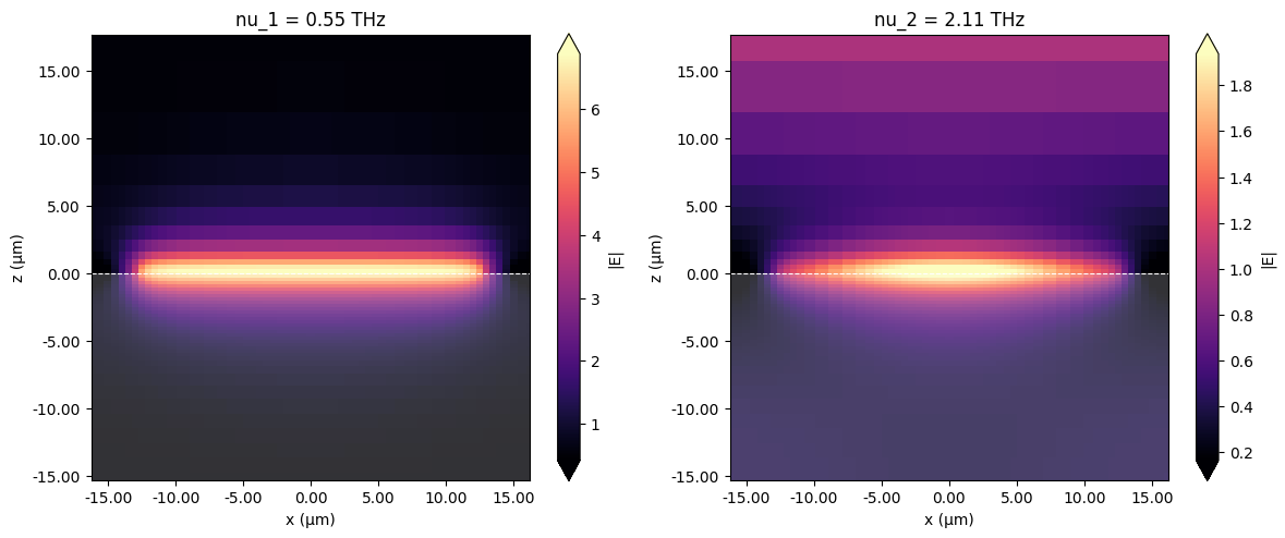
The confinement depth read off this cut is the design constraint that matters for the experiment. The mode is bound to the metal surface and decays into the GaAs over a scale set by the slot dimensions - tens of micrometers at most - rather than by the free-space wavelength of several hundred micrometers. That mismatch is exactly the sub-wavelength confinement that makes $\Omega_\mathrm{R}/\omega_\mathrm{c} > 1$ attainable.


 TERMS & CONDITIONS


 How the process works:
 Try this real URL to see an example: