Authors: Kristina Malinowski, Caltech; Amir Targholizadeh, Syracuse
Note: running the full notebook costs over 39 FlexCredits.
Many exciting frontiers in nanophotonics require the incorporation of materials beyond silicon or silicon nitride-based photonics, such as materials with specialized thermo-optic, electro-optic, photon emission, or photon absorption effects. When it is impractical to use these materials for homogeneous integration, we turn to hybrid nanophotonics. Hybrid nanophotonics often requires integrating these heterogeneous components with high coupling coefficients. We can use FDTD to model how these materials interact and optimize for the greatest possible coupling coefficients.
This notebook explores the design and optimization of an emitter-containing hexagonal boron nitride (hBN) nanowaveguide as a photon source and NbTiN as a superconducting photon detector, both integrated on a silicon nitride waveguide. In the work Malinowski, K., Targholizadeh, A. et al. Overcoming the Classical Signal to Noise Ratio Limit Through On-Chip Photon Addition. APL Quantum 3, 026107 (2026) DOI: 10.1063/5.0314599, we use FDTD to investigate the parameters driving maximal coupling between an hBN nanowaveguide and a silicon nitride waveguide and find the optimal nanowaveguide taper to couple a single-photon emitter in hexagonal boron nitride. Similarly, we study the parameters driving photon coupling from the silicon nitride waveguide to the NbTiN detector. The paper explores how a waveguide-coupled single-photon source and detector can be leveraged through single-photon addition for signal-to-noise amplification.
In this notebook, we reproduce the results presented in Fig. 2, Fig. 4, Fig. S2, and Fig. S3 of the paper and discuss the robustness of the nanowaveguide to deviations between the designed and fabricated devices.
First, we import the libraries needed for the simulations.
import tidy3d as td
import tidy3d.web as web
from tidy3d.plugins.mode import ModeSolver
10:47:53 -03 WARNING: Using canonical configuration directory at
             '/home/filipe/.config/tidy3d'. Found legacy directory at
             '~/.tidy3d', which will be ignored. Remove it manually or run
             'tidy3d config migrate --delete-legacy' to clean up.
/home/filipe/anaconda3/lib/python3.11/site-packages/trimesh/grouping.py:15: UserWarning: A NumPy version >=1.26.4 and <2.7.0 is required for this version of SciPy (detected version 1.26.1)
  from scipy.spatial import cKDTree
10:47:54 -03 ERROR: Failed to apply Tidy3D plotting style on import. Error:
             'tidy3d.style' not found in the style library and input is not a
             valid URL or path; see `style.available` for list of available
             styles
import matplotlib.pyplot as plt
import numpy as np
from tidy3d.plugins.dispersion import FastDispersionFitter, AdvancedFastFitterParam


from pylab import *
hBN Nanowaveguide Simulation
We start by defining the parameters that remain constant across the hBN nanowaveguide simulations.
# Define source wavelength in um and frequency in Hz
lambda_beg = 0.584
lambda_end = 0.586
freq_beg = td.C_0 / lambda_end
freq_end = td.C_0 / lambda_beg
freq0 = (freq_beg + freq_end) / 2
fwidth = freq_end - freq0

# Constant waveguide and nanowaveguide paramters in um
waveguide_width = 0.4
nwg_straight = 10
nwg_width = 0.31
sub_thickness = 5
dipole_height = 0.005  # measured from the waveguide-nanowaveguide interface

# Initial values for variable waveguide and nanowaveguide paramters
taper_length = 12  # um
taper_slope = (
    11 * 1e-3
)  # nm/um (for every 1 um along the length of the taper, the width of the taper decreases by x nm)
waveguide_thickness = 0.12  # um
nwg_thickness = 0.09  # um

# Import materials from Tidy3D library
SiO2 = td.material_library["SiO2"]["Horiba"]
Si3N4 = td.material_library["Si3N4"]["Philipp1973Sellmeier"]
vacuum = td.Medium(permittivity=1)
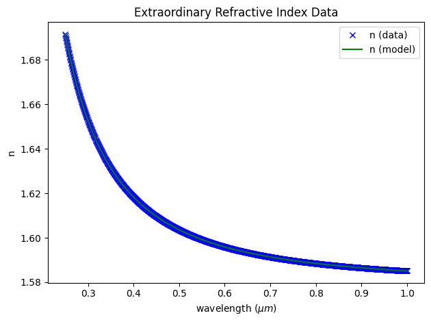
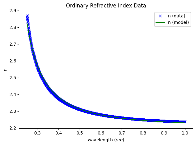
To model the anisotropic hBN, we use the dielectric functions and fitting parameters from Segura, A. et al. Natural optical anisotropy of h-BN: Highest giant birefringence in a bulk crystal through the mid-infrared to ultraviolet range. Phys. Rev. Materials 2, 024001 (2018). DOI: 10.1103/PhysRevMaterials.2.024001. The extraordinary refractive index is described by a simple Phillips-van Vechten model, and the ordinary refractive index by a Phillips-van Vechten model with an additional Lorentzian term that captures the excitonic transition contribution.
We fit the ordinary and extraordinary indices separately with the FastDispersionFitter and then assemble them as the diagonal terms of an AnisotropicMedium.
# Custom anisotropic hBN medium for 585 nm wavelength

# Initialize wavelength and wavenumber points
wavelengths = np.linspace(0.25, 1, 1000)  # Wavelength range in um
wavenumber = 1e4 / wavelengths

# Extraordinary Axis

# Define fitting parameters from paper
A = 110000  # sigma P0 para
B = 90000  # #sigma 0 para

# Generate data points
n_data = np.array((1 + A**2 / (B**2 - (wavenumber**2))) ** (1 / 2))

# Fit
advanced_param = AdvancedFastFitterParam(weights=(1, 1), num_iters=100)
fitter = FastDispersionFitter(wvl_um=wavelengths, n_data=n_data, wvl_range=(0.25, 1))
hbn_zz, rms_error = fitter.fit(
    max_num_poles=3, tolerance_rms=5e-2, eps_inf=1.0, advanced_param=advanced_param
)


# Plot
fitter.plot(hbn_zz)
plt.xlabel("wavelength ($\mu m$)")
plt.ylabel("n")
plt.title("Extraordinary Refractive Index Data")
plt.legend()
plt.show()

# Ordinary Axis

# Define fitting parameters from paper
C = 124100  # sigma P0 perp
D = 75100  # #sigma 0 perp
E = 53200  # sigma P1 perp
F = 49200  # sigma 1 perp
G = 1560  # gamma 1 perp

# Generate data points
n_data = np.array(
    (
        1
        + (C**2 / (D**2 - (wavenumber**2)))
        + (
            (E**2 * (F**2 - wavenumber**2))
            / ((F**2 - wavenumber**2) ** 2 + (G**2 * wavenumber**2))
        )
    )
    ** (1 / 2)
)


advanced_param = AdvancedFastFitterParam(weights=(1, 1), num_iters=100)
fitter = FastDispersionFitter(wvl_um=wavelengths, n_data=n_data, wvl_range=(0.25, 1))
hbn_xx, rms_error = fitter.fit(
    max_num_poles=3, tolerance_rms=5e-2, eps_inf=1.0, advanced_param=advanced_param
)

fitter.plot(hbn_xx)
plt.xlabel("wavelength ($\mu m$)")
plt.ylabel("n")
plt.title("Ordinary Refractive Index Data")
plt.legend()
plt.show()

hBN_ani = td.AnisotropicMedium(name="hBN_ani", xx=hbn_xx, yy=hbn_xx, zz=hbn_zz)
Output()
Output()
Design Simulation for a Tapered hBN Nanowaveguide with Variable hBN and Si3N4 Thickness
We build the simulation used to sweep the hBN and Si3N4 film thicknesses. The structure combines a Box for the Si3N4 waveguide and substrate with a PolySlab for the tapered hBN nanowaveguide, excited by a PointDipole source. Two ModeMonitor planes capture the power in the nanowaveguide mode and the Si3N4 waveguide mode, while a FluxMonitor normalizes by the emitted dipole power.
def Nanowaveguide_sim_thick(waveguide_thickness, nwg_thickness):

    # Set up simulation region size
    x_domain_size = (nwg_straight / 2 + taper_length + 2) * 2
    y_domain_size = 4 * waveguide_width
    z_domain_size = 1

    # Set up dipole source with TE polarization
    dipole = td.PointDipole(
        name="dipole",
        center=(0, 0, waveguide_thickness / 2 + dipole_height),
        source_time=td.GaussianPulse(
            freq0=freq0,
            fwidth=fwidth,
        ),
        polarization="Ey",
    )

    # Set up flux monitor for dipole power normalixation
    flux_dip = td.FluxMonitor(
        center=(0, 0, 0),
        size=(0.8 * x_domain_size, 0.8 * y_domain_size, 0.8 * z_domain_size),
        freqs=np.linspace(freq_beg, freq_end, 11),
        name="flux_dip",
    )

    # Set up mode monitor to measure power emitted into fundamental mode shared nanowaveguide and waveguide
    Nwg_mode = td.ModeMonitor(
        name="Nwg_mode",
        center=[(nwg_straight / 2) - 1, 0, 0],
        size=[0, td.inf, td.inf],
        freqs=np.linspace(freq_beg, freq_end, 11),
        mode_spec=td.ModeSpec(num_modes=1),
    )

    # Set up mode monitor to measure power coupled into fundamental waveguide mode
    Wg_mode = td.ModeMonitor(
        name="Wg_mode",
        center=[nwg_straight / 2 + taper_length + 1, 0, 0],
        size=[0, td.inf, td.inf],
        freqs=np.linspace(freq_beg, freq_end, 11),
        mode_spec=td.ModeSpec(num_modes=1),
    )

    # Set up waveguide structure
    Waveguide = td.Structure(
        name="Waveguide",
        geometry=td.Box(size=[td.inf, waveguide_width, waveguide_thickness]),
        medium=Si3N4,
    )

    # Set up substrate structure
    Substrate = td.Structure(
        geometry=td.Box(
            center=[0, 0, -sub_thickness / 2 - waveguide_thickness / 2],
            size=[td.inf, td.inf, sub_thickness],
        ),
        name="Substrate",
        medium=SiO2,
    )

    # Set up nanowaveguide structure. NOTE: If the taper length and slope are such that the nanowaveguide end in a single point, an error will occur.
    Nanowaveguide = td.Structure(
        geometry=td.PolySlab(
            slab_bounds=[
                waveguide_thickness / 2,
                waveguide_thickness / 2 + nwg_thickness,
            ],
            vertices=[
                [
                    -nwg_straight / 2 - taper_length,
                    nwg_width / 2 - taper_slope * taper_length,
                ],
                [-nwg_straight / 2, nwg_width / 2],
                [nwg_straight / 2, nwg_width / 2],
                [
                    nwg_straight / 2 + taper_length,
                    nwg_width / 2 - taper_slope * taper_length,
                ],
                [
                    nwg_straight / 2 + taper_length,
                    -(nwg_width / 2 - taper_slope * taper_length),
                ],
                [nwg_straight / 2, -nwg_width / 2],
                [-nwg_straight / 2, -nwg_width / 2],
                [
                    -nwg_straight / 2 - taper_length,
                    -(nwg_width / 2 - taper_slope * taper_length),
                ],
            ],
        ),
        name="Nanowaveguide",
        medium=hBN_ani,
    )

    # Create simulation
    min_steps_per_wvl = 8
    run_time = 1e-11
    shutoff = 5e-5

    sim = td.Simulation(
        size=[x_domain_size, y_domain_size, z_domain_size],
        center=(0, 0, 0),
        run_time=run_time,
        shutoff=shutoff,
        grid_spec=td.GridSpec.auto(
            min_steps_per_wvl=min_steps_per_wvl, wavelength=td.C_0 / freq0
        ),
        medium=vacuum,
        sources=[dipole],
        monitors=[Nwg_mode, Wg_mode, flux_dip],
        structures=[Waveguide, Substrate, Nanowaveguide],
    )

    return sim
# Define the sweep
waveguide_thickness_sweep = np.linspace(0.08, 0.14, 13)
nwg_thickness_sweep = np.linspace(0.04, 0.12, 9)

# Define the path to save data
path = "data/20260122 thickness sweep/"

# Build the simulation batch
sims_thick = {
    f"wg_thickness={wgt * 1e3:.3f}nm;nwg_thickness={nwgt * 1e3:.3f}nm": Nanowaveguide_sim_thick(
        wgt, nwgt
    )
    for wgt in waveguide_thickness_sweep
    for nwgt in nwg_thickness_sweep
}

# Run the simulation batch
batch_thick = web.Batch(simulations=sims_thick)
est_fc = batch_thick.estimate_cost()
batch_thick_results = batch_thick.run(path_dir=path)
real_fc = batch_thick.real_cost()
10:58:24 -03 Maximum FlexCredit cost: 40.761 for the whole batch.
Output()
10:58:31 -03 Started working on Batch containing 117 tasks.
11:01:58 -03 Maximum FlexCredit cost: 40.761 for the whole batch.
             Use 'Batch.real_cost()' to get the billed FlexCredit cost after
             completion.
Output()
11:09:13 -03 Batch complete.
11:11:13 -03 Total billed flex credit cost: 7.831.
# Analyze the results

# Uncomment below to load from file
# batch_thick = web.Batch.from_file("data/20260122 thickness sweep/batch.hdf5")
# batch_thick_results = batch_thick.load("data/20260122 thickness sweep/")

# Define arrays
Nwg_mode_thick = np.zeros([len(nwg_thickness_sweep), len(waveguide_thickness_sweep)])
Wg_mode_thick = np.zeros([len(nwg_thickness_sweep), len(waveguide_thickness_sweep)])

# Populate data arrays with coupling coefficients averaged across simulated frequencies and normalized by the dipole source power
for i in range(len(waveguide_thickness_sweep)):
    for j in range(len(nwg_thickness_sweep)):
        wgt = waveguide_thickness_sweep[i]
        nwgt = nwg_thickness_sweep[j]
        dipole_power = np.mean(
            batch_thick_results[
                f"wg_thickness={wgt * 1e3:.3f}nm;nwg_thickness={nwgt * 1e3:.3f}nm"
            ]["flux_dip"].flux
        )
        norm_coup_nwg = (
            np.mean(
                np.abs(
                    batch_thick_results[
                        f"wg_thickness={wgt * 1e3:.3f}nm;nwg_thickness={nwgt * 1e3:.3f}nm"
                    ]["Nwg_mode"].amps.sel(direction="+")
                )
                ** 2
            )
            / dipole_power
        )
        norm_coup_wg = (
            np.mean(
                np.abs(
                    batch_thick_results[
                        f"wg_thickness={wgt * 1e3:.3f}nm;nwg_thickness={nwgt * 1e3:.3f}nm"
                    ]["Wg_mode"].amps.sel(direction="+")
                )
                ** 2
            )
            / dipole_power
        )
        Nwg_mode_thick[j][i] = norm_coup_nwg
        Wg_mode_thick[j][i] = norm_coup_wg


# Coupling through the taper between light in the nanowaveguide mode and the waveguide mode found using the ratio of the total coupling in the two modes
Nwg_Wg_coup_thick = Wg_mode_thick / Nwg_mode_thick

# Redefine ticks in nm for plotting
wg_tick = np.linspace(80, 140, 7)
nwg_tick = np.linspace(40, 120, 9)

# Initialize figure
fig, axs = plt.subplots(3, 1)
fig.tight_layout()
fig.set_size_inches(6, 18)
fig.set_dpi(300)
c_map = cm.get_cmap("plasma")

# Plot data arrays
im1 = axs[0].imshow(
    Nwg_mode_thick,
    interpolation="none",
    cmap=c_map,
    aspect="auto",
    extent=[77.5, 142.5, 125, 35],
)
im2 = axs[1].imshow(
    Nwg_Wg_coup_thick,
    interpolation="none",
    cmap=c_map,
    aspect="auto",
    extent=[77.5, 142.5, 125, 35],
)
im3 = axs[2].imshow(
    Wg_mode_thick,
    interpolation="none",
    cmap=c_map,
    aspect="auto",
    extent=[77.5, 142.5, 125, 35],
)

# Figure formating for emitter to nanowaveguide coupling analysis
axs[0].set_title("Emitter to Nanowaveguide - Coupling Coefficient", fontsize=18)
axs[0].set_ylabel("hBN  Thickness (nm)", fontsize=18)
axs[0].set_xlabel("Si3N4 Thickness (nm)", fontsize=18)
axs[0].set_xticks(wg_tick)
axs[0].set_yticks(nwg_tick)
axs[0].tick_params(which="major", direction="in", length=8)
axs[0].tick_params(which="minor", direction="in", length=4)
axs[0].tick_params(axis="both", labelsize=18, pad=5)
axs[0].set_ylabel("hBN  Thickness (nm)", fontsize=18)
axs[0].set_xlabel("Si3N4 Thickness (nm)", fontsize=18)

cbar1 = plt.colorbar(im1)
cbar1.set_label("Coupling Coefficient", fontsize=18)
cbar1.ax.tick_params(labelsize=18)

# Figure formating for emitter to nanowaveguide coupling analysis
axs[1].set_title("Nanowaveguide to Waveguide - Coupling Coefficient", fontsize=18)
axs[1].set_xticks(wg_tick)
axs[1].set_yticks(nwg_tick)
axs[1].tick_params(which="major", direction="in", length=8)
axs[1].tick_params(which="minor", direction="in", length=4)
axs[1].tick_params(axis="both", labelsize=18, pad=5)
axs[1].set_ylabel("hBN  Thickness (nm)", fontsize=18)
axs[1].set_xlabel("Si3N4 Thickness (nm)", fontsize=18)

cbar2 = plt.colorbar(im2)
cbar2.set_label("Coupling Coefficient", fontsize=18)
cbar2.ax.tick_params(labelsize=18)

# Figure formating for emitter to nanowaveguide coupling analysis
axs[2].set_title("Total Waveguide - Coupling Coefficient", fontsize=18)
axs[2].set_xticks(wg_tick)
axs[2].set_yticks(nwg_tick)
axs[2].tick_params(which="major", direction="in", length=8)
axs[2].tick_params(which="minor", direction="in", length=4)
axs[2].tick_params(axis="both", labelsize=18, pad=5)
axs[2].set_ylabel("hBN  Thickness (nm)", fontsize=18)
axs[2].set_xlabel("Si3N4 Thickness (nm)", fontsize=18)

cbar3 = plt.colorbar(im3)
cbar3.set_label("Coupling Coefficient", fontsize=18)
cbar3.ax.tick_params(labelsize=18)

plt.show()
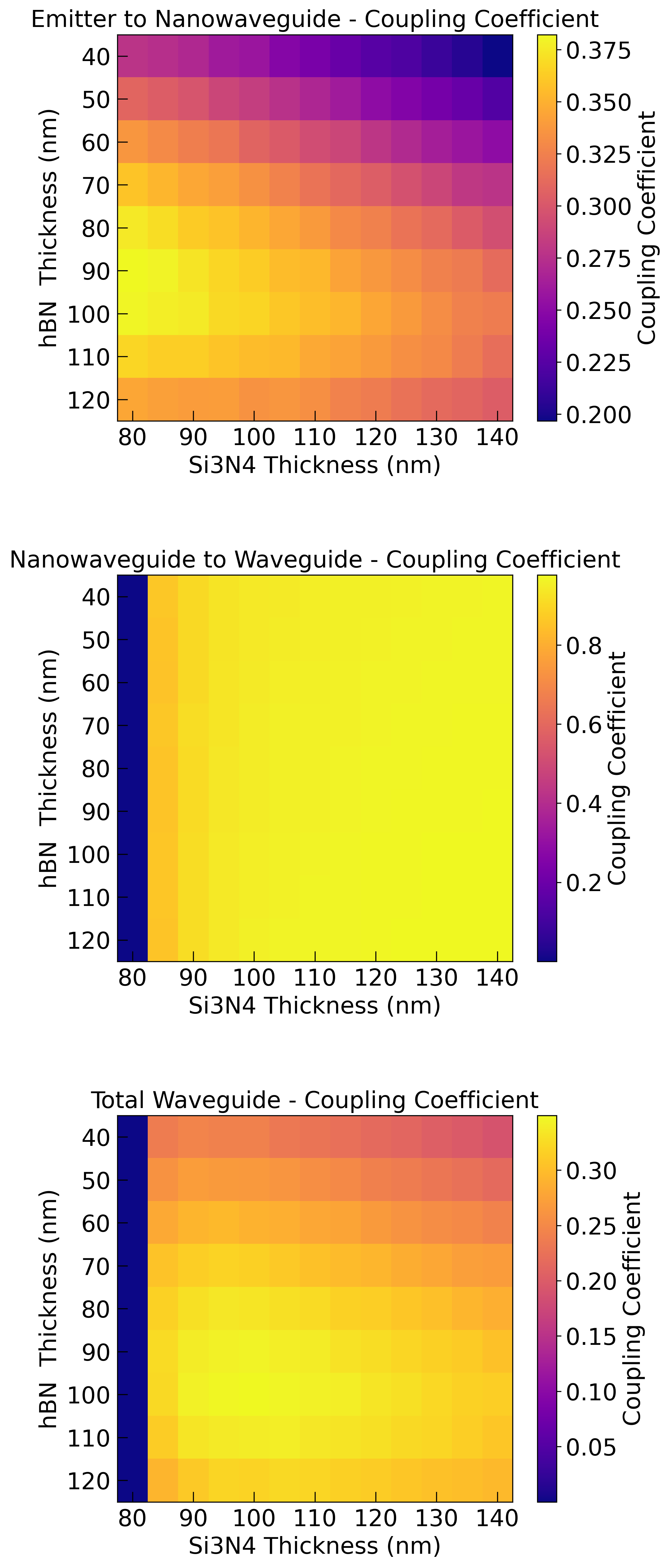
We pick the nanowaveguide and waveguide thicknesses that maximize the total coupling and use them in the following simulations.
max_flat_index = np.argmax(Wg_mode_thick)
nwg_ind, wg_ind = np.unravel_index(max_flat_index, Wg_mode_thick.shape)

max_wg = waveguide_thickness_sweep[wg_ind]
max_nwg = nwg_thickness_sweep[nwg_ind]
max_coup = Wg_mode_thick[nwg_ind][wg_ind]

print(
    f"Maximum total coupling of {max_coup:.3f} with {round(max_wg * 1e3)} nm thick waveguide and {round(max_nwg * 1e3)} nm thick nanowaveguide"
)  # Output: 89

waveguide_thickness = max_wg
# for these simulations we choose to overide the optimal waveguide thickness, for a slightly thicker waveguide because it benefits racetrack resonator coupling for the full device investigate in the companion paper
waveguide_thickness = 0.12  # um
nwg_thickness = max_nwg
Maximum total coupling of 0.349 with 100 nm thick waveguide and 100 nm thick nanowaveguide
Design Simulation for a Tapered hBN Nanowaveguide with Variable Taper Length and Slope
We now build the simulation that sweeps the taper length and slope of the nanowaveguide.
def Nanowaveguide_sim_tap(taper_length, taper_slope):

    # Set up simulation region size
    x_domain_size = (nwg_straight / 2 + taper_length + 2) * 2
    y_domain_size = 4 * waveguide_width
    z_domain_size = 1

    # Set up dipole source with TE polarization
    dipole = td.PointDipole(
        name="dipole",
        center=(0, 0, waveguide_thickness / 2 + dipole_height),
        source_time=td.GaussianPulse(
            freq0=freq0,
            fwidth=fwidth,
        ),
        polarization="Ey",
    )

    # Set up flux monitor for dipole power normalixation
    flux_dip = td.FluxMonitor(
        center=(0, 0, 0),
        size=(0.8 * x_domain_size, 0.8 * y_domain_size, 0.8 * z_domain_size),
        freqs=np.linspace(freq_beg, freq_end, 11),
        name="flux_dip",
    )

    # Set up mode monitor to measure power emitted into fundamental mode shared nanowaveguide and waveguide
    Nwg_mode = td.ModeMonitor(
        name="Nwg_mode",
        center=[(nwg_straight / 2) - 1, 0, 0],
        size=[0, td.inf, td.inf],
        freqs=np.linspace(freq_beg, freq_end, 11),
        mode_spec=td.ModeSpec(num_modes=1),
    )

    # Set up mode monitor to measure power coupled into fundamental waveguide mode
    Wg_mode = td.ModeMonitor(
        name="Wg_mode",
        center=[nwg_straight / 2 + taper_length + 1, 0, 0],
        size=[0, td.inf, td.inf],
        freqs=np.linspace(freq_beg, freq_end, 11),
        mode_spec=td.ModeSpec(num_modes=1),
    )

    # Set up waveguide structure
    Waveguide = td.Structure(
        name="Waveguide",
        geometry=td.Box(size=[td.inf, waveguide_width, waveguide_thickness]),
        medium=Si3N4,
    )

    # Set up substrate structure
    Substrate = td.Structure(
        geometry=td.Box(
            center=[0, 0, -sub_thickness / 2 - waveguide_thickness / 2],
            size=[td.inf, td.inf, sub_thickness],
        ),
        name="Substrate",
        medium=SiO2,
    )

    # Set up nanowaveguide structure. NOTE: If the taper length and slope are such that the nanowaveguide end in a single point, an error will occur.
    Nanowaveguide = td.Structure(
        geometry=td.PolySlab(
            slab_bounds=[
                waveguide_thickness / 2,
                waveguide_thickness / 2 + nwg_thickness,
            ],
            vertices=[
                [
                    -nwg_straight / 2 - taper_length,
                    nwg_width / 2 - taper_slope * taper_length,
                ],
                [-nwg_straight / 2, nwg_width / 2],
                [nwg_straight / 2, nwg_width / 2],
                [
                    nwg_straight / 2 + taper_length,
                    nwg_width / 2 - taper_slope * taper_length,
                ],
                [
                    nwg_straight / 2 + taper_length,
                    -(nwg_width / 2 - taper_slope * taper_length),
                ],
                [nwg_straight / 2, -nwg_width / 2],
                [-nwg_straight / 2, -nwg_width / 2],
                [
                    -nwg_straight / 2 - taper_length,
                    -(nwg_width / 2 - taper_slope * taper_length),
                ],
            ],
        ),
        name="Nanowaveguide",
        medium=hBN_ani,
    )

    # Create simulation
    min_steps_per_wvl = 6
    run_time = 1e-11
    shutoff = 5e-5

    sim = td.Simulation(
        size=[x_domain_size, y_domain_size, z_domain_size],
        center=(0, 0, 0),
        run_time=run_time,
        shutoff=shutoff,
        grid_spec=td.GridSpec.auto(
            min_steps_per_wvl=min_steps_per_wvl, wavelength=td.C_0 / freq0
        ),
        medium=vacuum,
        sources=[dipole],
        monitors=[Nwg_mode, Wg_mode, flux_dip],
        structures=[Waveguide, Substrate, Nanowaveguide],
    )

    return sim
Run the Taper Sweep
We launch the taper sweep as a batch and analyze the data.
# Define the sweep
taper_length_sweep = np.linspace(1, 50, 50)
taper_slope_sweep = np.linspace(1e-3, 30e-3, 30)

# Define the path to save data
path = "data/20260126 taper sweep/"

# Build the simulation batch. We include an if statement to filter out invalid cases where the taper length is too long for larger taper slopes resulting in invalid polygons.
sims_tap = {
    f"taper_length={tl:.3f}um;taper_slope={ts * 1e3:.3f}": Nanowaveguide_sim_tap(tl, ts)
    for tl in taper_length_sweep
    for ts in taper_slope_sweep
    if (nwg_width / 2 - ts * tl) > 0
}
# Run the simulation batch
batch_tap = web.Batch(simulations=sims_tap)
est_fc = batch_tap.estimate_cost()
batch_tap_results = batch_tap.run(path_dir=path)
real_fc = batch_tap.real_cost()
11:57:10 -03 Maximum FlexCredit cost: 97.690 for the whole batch.
Output()
11:57:42 -03 Started working on Batch containing 472 tasks.
12:11:12 -03 Maximum FlexCredit cost: 97.690 for the whole batch.
             Use 'Batch.real_cost()' to get the billed FlexCredit cost after
             completion.
Output()
12:33:14 -03 Batch complete.
12:41:17 -03 Total billed flex credit cost: 24.278.
# Analyze the results

# Uncomment below to load from file
# batch_tap = web.Batch.from_file("data/20260126 taper sweep/batch.hdf5")
# batch_tap_results = batch_tap.load("data/20260126 taper sweep/")

# Define arrays
Nwg_mode_tap = np.zeros([len(taper_slope_sweep), len(taper_length_sweep)])
Wg_mode_tap = np.zeros([len(taper_slope_sweep), len(taper_length_sweep)])

# Populate data arrays with coupling coefficients averaged across simulated frequencies and normalized by the dipole source power
for i in range(len(taper_length_sweep)):
    for j in range(len(taper_slope_sweep)):
        tl = taper_length_sweep[i]
        ts = taper_slope_sweep[j]
        if (nwg_width / 2 - ts * tl) > 0:
            dipole_power = np.mean(
                batch_tap_results[
                    f"taper_length={tl:.3f}um;taper_slope={ts * 1e3:.3f}"
                ]["flux_dip"].flux
            )
            norm_coup_nwg = (
                np.mean(
                    np.abs(
                        batch_tap_results[
                            f"taper_length={tl:.3f}um;taper_slope={ts * 1e3:.3f}"
                        ]["Nwg_mode"].amps.sel(direction="+")
                    )
                    ** 2
                )
                / dipole_power
            )
            norm_coup_wg = (
                np.mean(
                    np.abs(
                        batch_tap_results[
                            f"taper_length={tl:.3f}um;taper_slope={ts * 1e3:.3f}"
                        ]["Wg_mode"].amps.sel(direction="+")
                    )
                    ** 2
                )
                / dipole_power
            )
            Nwg_mode_tap[j][i] = norm_coup_nwg
            Wg_mode_tap[j][i] = norm_coup_wg

# Redefine ticks in nm for plotting
len_tick = [1, 5, 10, 15, 20, 25, 30, 35, 40, 45, 50]
slope_tick = np.linspace(2e-3, 30e-3, 15) * 1e3

# Initialize figure
fig, axs = plt.subplots(3, 1)
fig.tight_layout()
fig.set_size_inches(6, 18)
fig.set_dpi(300)
c_map = cm.get_cmap("plasma")

# Set invalid taper length and slope combinations to NaN in array and white on plot
c_map.set_bad("white")
Nwg_mode_tap_copy = Nwg_mode_tap.copy()
Nwg_mode_tap[Nwg_mode_tap == 0] = np.nan
Wg_mode_tap_copy = Wg_mode_tap.copy()
Wg_mode_tap[Wg_mode_tap == 0] = np.nan

# Coupling through the taper between light in the nanowaveguide mode and the waveguide mode found using the ratio of the total coupling in the two modes
Nwg_Wg_coup_tap = Wg_mode_tap / Nwg_mode_tap

# Plot data arrays
im1 = axs[0].imshow(
    Nwg_mode_tap,
    interpolation="none",
    cmap=c_map,
    aspect="auto",
    extent=[0.5, 50.5, 30.5, 0.5],
)
im2 = axs[1].imshow(
    Nwg_Wg_coup_tap,
    interpolation="none",
    cmap=c_map,
    aspect="auto",
    extent=[0.5, 50.5, 30.5, 0.5],
)
im3 = axs[2].imshow(
    Wg_mode_tap,
    interpolation="none",
    cmap=c_map,
    aspect="auto",
    extent=[0.5, 50.5, 30.5, 0.5],
)

# Figure formating for emitter to nanowaveguide coupling analysis
axs[0].set_title("Emitter to Nanowaveguide - Coupling Coefficient", fontsize=18)
axs[0].set_ylabel("hBN  Thickness (nm)", fontsize=18)
axs[0].set_xlabel("Si3N4 Thickness (nm)", fontsize=18)
axs[0].set_xticks(len_tick)
axs[0].set_yticks(slope_tick)
axs[0].tick_params(which="major", direction="in", length=8)
axs[0].tick_params(which="minor", direction="in", length=4)
axs[0].tick_params(axis="both", labelsize=18, pad=5)
axs[0].set_ylabel("Taper Slope (nm/$\mu m$)", fontsize=18)
axs[0].set_xlabel("Taper Length ($\mu m$)", fontsize=18)

cbar1 = plt.colorbar(im1)
cbar1.set_label("Coupling Coefficient", fontsize=18)
cbar1.ax.tick_params(labelsize=18)

# Figure formating for emitter to nanowaveguide coupling analysis
axs[1].set_title("Nanowaveguide to Waveguide - Coupling Coefficient", fontsize=18)
axs[1].set_xticks(len_tick)
axs[1].set_yticks(slope_tick)
axs[1].tick_params(which="major", direction="in", length=8)
axs[1].tick_params(which="minor", direction="in", length=4)
axs[1].tick_params(axis="both", labelsize=18, pad=5)
axs[1].set_ylabel("Taper Slope (nm/$\mu m$)", fontsize=18)
axs[1].set_xlabel("Taper Length ($\mu m$)", fontsize=18)

cbar2 = plt.colorbar(im2)
cbar2.set_label("Coupling Coefficient", fontsize=18)
cbar2.ax.tick_params(labelsize=18)

# Figure formating for emitter to nanowaveguide coupling analysis
axs[2].set_title("Total Waveguide - Coupling Coefficient", fontsize=18)
axs[2].set_xticks(len_tick)
axs[2].set_yticks(slope_tick)
axs[2].tick_params(which="major", direction="in", length=8)
axs[2].tick_params(which="minor", direction="in", length=4)
axs[2].tick_params(axis="both", labelsize=18, pad=5)
axs[2].set_ylabel("Taper Slope (nm/$\mu m$)", fontsize=18)
axs[2].set_xlabel("Taper Length ($\mu m$)", fontsize=18)

cbar3 = plt.colorbar(im3)
cbar3.set_label("Coupling Coefficient", fontsize=18)
cbar3.ax.tick_params(labelsize=18)

plt.show()
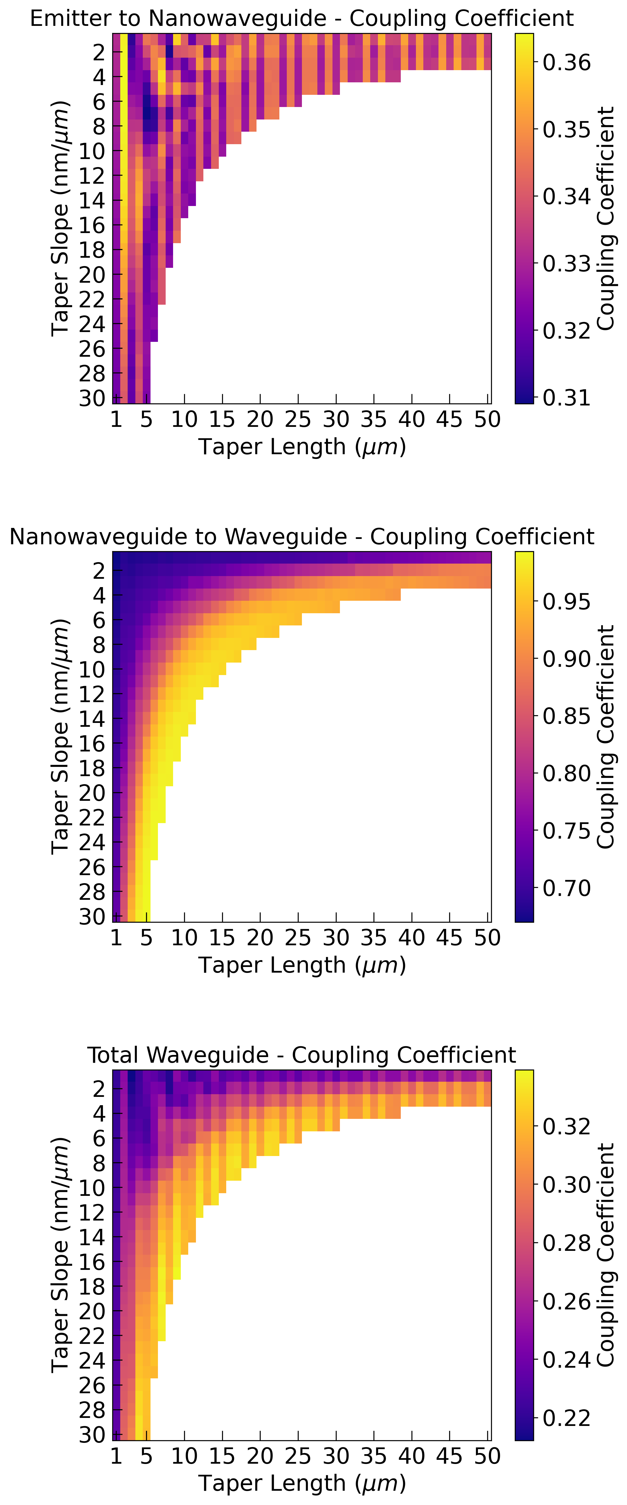
As before, we pick the taper length and slope that maximize the total coupling and use them in the following simulations.
max_flat_index = np.nanargmax(Wg_mode_tap)
ts_ind, tl_ind = np.unravel_index(max_flat_index, Wg_mode_tap.shape)

max_tl = taper_length_sweep[tl_ind]
max_ts = taper_slope_sweep[ts_ind]
max_coup = Wg_mode_tap[ts_ind][tl_ind]

print(
    f"Maximum total coupling of {max_coup:.3f} with {max_tl} um taper length and {max_ts * 1e3:.1f} nm/um taper slope"
)  # Output: 89

taper_length = max_tl
taper_slope = max_ts
Maximum total coupling of 0.339 with 9.0 um taper length and 17.0 nm/um taper slope
High-Resolution Simulation
With the nanowaveguide geometry optimized, we run a single high-resolution simulation to inspect the mode profiles and the mode transformation along the taper. We add two ModeSolver monitors at the input and output planes and a FieldMonitor along the taper after the dipole.
def Nanowaveguide_sim_hires():
# Set up simulation region size
x_domain_size = (nwg_straight / 2 + taper_length + 2) * 2
y_domain_size = 4 * waveguide_width
z_domain_size = 1
# Set up dipole source with TE polarization
dipole = td.PointDipole(
name="dipole",
center=(0, 0, waveguide_thickness / 2 + dipole_height),
source_time=td.GaussianPulse(
freq0=freq0,
fwidth=fwidth,
),
polarization="Ey",
)
# Set up flux monitor for dipole power normalixation
flux_dip = td.FluxMonitor(
center=(0, 0, 0),
size=(0.8 * x_domain_size, 0.8 * y_domain_size, 0.8 * z_domain_size),
freqs=np.linspace(freq_beg, freq_end, 11),
name="flux_dip",
)
# Set up mode monitor to measure power emitted into fundamental mode shared nanowaveguide and waveguide
Nwg_mode = td.ModeMonitor(
name="Nwg_mode",
center=[(nwg_straight / 2) - 1, 0, 0],
size=[0, td.inf, td.inf],
freqs=np.linspace(freq_beg, freq_end, 11),
mode_spec=td.ModeSpec(num_modes=1),
)
# Set up mode monitor to measure power coupled into fundamental waveguide mode
Wg_mode = td.ModeMonitor(
name="Wg_mode",
center=[nwg_straight / 2 + taper_length + 1, 0, 0],
size=[0, td.inf, td.inf],
freqs=np.linspace(freq_beg, freq_end, 11),
mode_spec=td.ModeSpec(num_modes=1),
)
# Set up waveguide structure
Waveguide = td.Structure(
name="Waveguide",
geometry=td.Box(size=[td.inf, waveguide_width, waveguide_thickness]),
medium=Si3N4,
)
# Set up substrate structure
Substrate = td.Structure(
geometry=td.Box(
center=[0, 0, -sub_thickness / 2 - waveguide_thickness / 2],
size=[td.inf, td.inf, sub_thickness],
),
name="Substrate",
medium=SiO2,
)
# Set up nanowaveguide structure. NOTE: If the taper length and slope are such that the nanowaveguide end in a single point, an error will occur.
Nanowaveguide = td.Structure(
geometry=td.PolySlab(
slab_bounds=[
waveguide_thickness / 2,
waveguide_thickness / 2 + nwg_thickness,
],
vertices=[
[
-nwg_straight / 2 - taper_length,
nwg_width / 2 - taper_slope * taper_length,
],
[-nwg_straight / 2, nwg_width / 2],
[nwg_straight / 2, nwg_width / 2],
[
nwg_straight / 2 + taper_length,
nwg_width / 2 - taper_slope * taper_length,
],
[
nwg_straight / 2 + taper_length,
-(nwg_width / 2 - taper_slope * taper_length),
],
[nwg_straight / 2, -nwg_width / 2],
[-nwg_straight / 2, -nwg_width / 2],
[
-nwg_straight / 2 - taper_length,
-(nwg_width / 2 - taper_slope * taper_length),
],
],
),
name="Nanowaveguide",
medium=hBN_ani,
)
# Set up field monitor
field_monitor = td.FieldMonitor(
center=(x_domain_size / 4 + 0.1, 0, 0),
size=(x_domain_size / 2, 0, td.inf),
freqs=[
freq0
], # NOTE: small offset in the center x-coordinate prevents dipole source from drowning out the field in the taper
name="field",
)
# Create simulation
min_steps_per_wvl = 20
run_time = 1e-11
shutoff = 5e-5
sim = td.Simulation(
size=[x_domain_size, y_domain_size, z_domain_size],
center=(0, 0, 0),
run_time=run_time,
shutoff=shutoff,
grid_spec=td.GridSpec.auto(
min_steps_per_wvl=min_steps_per_wvl, wavelength=td.C_0 / freq0
),
medium=vacuum,
sources=[dipole],
monitors=[Nwg_mode, Wg_mode, flux_dip, field_monitor],
structures=[Waveguide, Substrate, Nanowaveguide],
)
mon_plane_nwg = td.Box(
center=[(nwg_straight / 2) - 1, 0, 0],
size=[0, 4 * waveguide_width, 4 * (waveguide_thickness + nwg_thickness)],
)
mode_spec = td.ModeSpec(num_modes=1)
ms_nwg = ModeSolver(
simulation=sim, plane=mon_plane_nwg, mode_spec=mode_spec, freqs=[freq0]
)
modes_nwg = ms_nwg.solve()
modes_nwg.to_dataframe()
mon_plane_wg = td.Box(
center=[nwg_straight / 2 + taper_length + 1, 0, 0],
size=[0, 4 * waveguide_width, 4 * (waveguide_thickness + nwg_thickness)],
)
mode_spec = td.ModeSpec(num_modes=1)
ms_wg = ModeSolver(
simulation=sim, plane=mon_plane_wg, mode_spec=mode_spec, freqs=[freq0]
)
modes_wg = ms_wg.solve()
modes_wg.to_dataframe()
fig, axs = plt.subplots(
2,
1,
)
fig.tight_layout()
fig.set_size_inches(8, 10)
Ex1 = modes_nwg.Ex
Ey1 = modes_nwg.Ey
Ez1 = modes_nwg.Ez
E1 = (abs(Ez1) ** 2 + abs(Ex1) ** 2 + abs(Ey1) ** 2) ** (1 / 2)
E1 = E1 / np.max(E1)
Ex2 = modes_wg.Ex
Ey2 = modes_wg.Ey
Ez2 = modes_wg.Ez
E2 = (abs(Ez2) ** 2 + abs(Ex2) ** 2 + abs(Ey2) ** 2) ** (1 / 2)
E2 = E2 / np.max(E2)
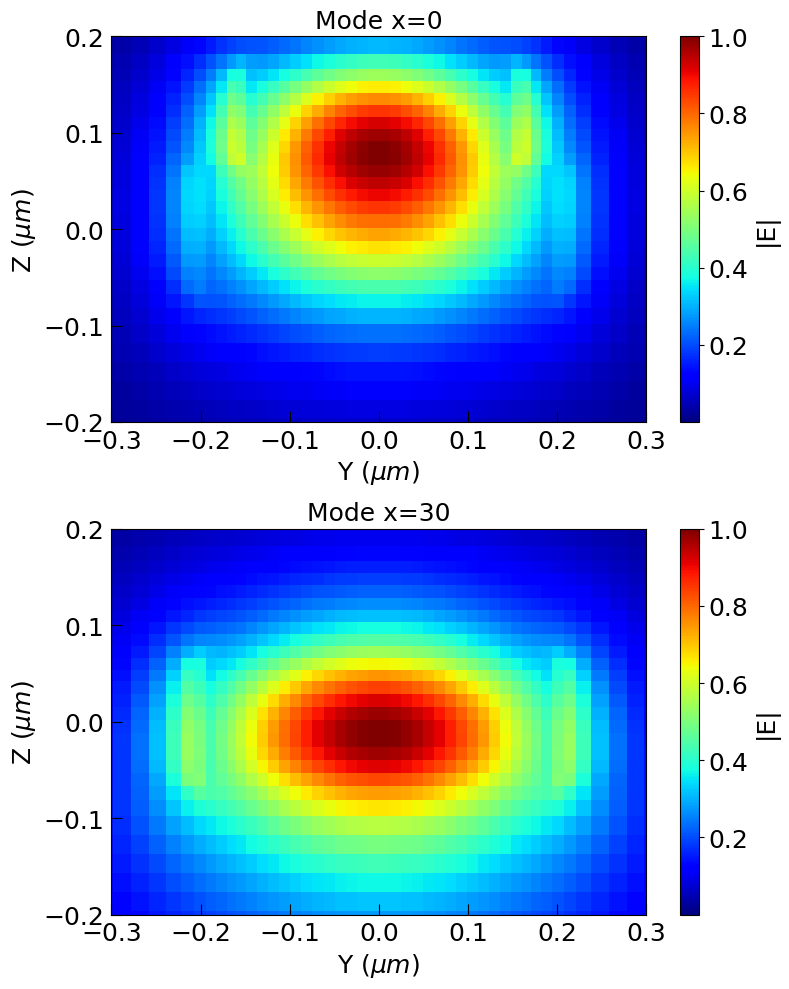
im1 = E1.plot(x="y", y="z", ax=axs[0], cmap="jet")
im2 = E2.plot(x="y", y="z", ax=axs[1], cmap="jet")
axs[0].set_title("Mode x=0", fontsize=18)
axs[1].set_title("Mode x=30", fontsize=18)
axs[0].set_ylabel("Z ($\mu m$)", fontsize=18)
axs[0].set_xlabel("Y ($\mu m$)", fontsize=18)
axs[1].set_ylabel("Z ($\mu m$)", fontsize=18)
axs[1].set_xlabel("Y ($\mu m$)", fontsize=18)
# axs[0].yaxis.set_minor_locator(AutoMinorLocator())
axs[0].tick_params(which="major", direction="in", length=8)
axs[0].tick_params(which="minor", direction="in", length=4)
axs[0].tick_params(axis="both", labelsize=18, pad=5)
axs[0].set_ylim(-0.2, 0.2)
axs[0].set_xlim(-0.3, 0.3)
# axs[1].yaxis.set_minor_locator(AutoMinorLocator())
axs[1].tick_params(which="major", direction="in", length=8)
axs[1].tick_params(which="minor", direction="in", length=4)
axs[1].tick_params(axis="both", labelsize=18, pad=5)
axs[1].set_ylim(-0.2, 0.2)
axs[1].set_xlim(-0.3, 0.3)
cbar1 = im1.colorbar
cbar1.set_label("|E|", fontsize=18)
cbar1.ax.tick_params(labelsize=18)
cbar2 = im2.colorbar
cbar2.set_label("|E|", fontsize=18)
cbar2.ax.tick_params(labelsize=18)
plt.tight_layout()
plt.show()
return sim
We plot the modes at the two monitor planes and run the high-resolution simulation.
path = "data/20260126 field profile/"

sim = Nanowaveguide_sim_hires()

name = (
    "Nanowaveguide_TL_"
    + str(int(taper_length))
    + "um_TS_"
    + str(round(taper_slope * 1e3))
    + "_wgT_"
    + str(round(waveguide_thickness * 1e3))
    + "nm_nwgT_"
    + str(round(nwg_thickness * 1e3))
    + "nm_hires"
)
job = web.Job(simulation=sim, task_name=name)
FC = web.estimate_cost(job.task_id)
path = path + name + ".hdf5"
sim_data = job.run(path=path)

time.sleep(2)
real_fc = web.real_cost(job.task_id)
13:00:13 -03 WARNING: Use the remote mode solver with subpixel averaging for
             better accuracy through 'tidy3d.web.run(...)' or the deprecated
             'tidy3d.plugins.mode.web.run(...)'.
/home/filipe/anaconda3/lib/python3.11/site-packages/scipy/sparse/_construct.py:543: FutureWarning: Input has data type int64, but the output has been cast to float64.  In the future, the output data type will match the input. To avoid this warning, set the `dtype` parameter to `None` to have the output dtype match the input, or set it to the desired output data type.
Note: In Python 3.11, this warning can be generated by a call of scipy.sparse.diags(), but the code indicated in the warning message will refer to an internal call of scipy.sparse.diags_array(). If that happens, check your code for the use of diags().
  A = diags_array(diagonals, offsets=offsets, shape=shape, dtype=dtype)
13:00:15 -03 Created task
             'Nanowaveguide_TL_9um_TS_17_wgT_120nm_nwgT_100nm_hires' with
             resource_id 'fdve-2da1ca7b-79ec-40ce-a772-ef15b20ae05f' and
             task_type 'FDTD'.
             View task using web UI at
             'https://tidy3d.simulation.cloud/workbench?taskId=fdve-2da1ca7b-79e
             c-40ce-a772-ef15b20ae05f'.
Task folder: 'default'.
Output()
13:00:20 -03 Estimated FlexCredit cost: 4.396. Minimum cost depends on task
             execution details. Use 'web.real_cost(task_id)' to get the billed
             FlexCredit cost after a simulation run.
13:00:22 -03 Estimated FlexCredit cost: 4.396. Minimum cost depends on task
             execution details. Use 'web.real_cost(task_id)' to get the billed
             FlexCredit cost after a simulation run.
13:00:26 -03 status = queued
             To cancel the simulation, use 'web.abort(task_id)' or
             'web.delete(task_id)' or abort/delete the task in the web UI.
             Terminating the Python script will not stop the job running on the
             cloud.
Output()
13:00:30 -03 status = preprocess
13:00:35 -03 starting up solver
13:00:36 -03 running solver
Output()
13:03:00 -03 early shutoff detected at 16%, exiting.
status = postprocess
Output()
13:03:04 -03 status = success
13:03:06 -03 View simulation result at
             'https://tidy3d.simulation.cloud/workbench?taskId=fdve-2da1ca7b-79e
             c-40ce-a772-ef15b20ae05f'.
Output()
13:03:11 -03 Loading simulation from data/20260126 field
             profile/Nanowaveguide_TL_9um_TS_17_wgT_120nm_nwgT_100nm_hires.hdf5
13:03:14 -03 Billed flex credit cost: 0.712.
             Note: the task cost pro-rated due to early shutoff was below the
             minimum threshold, due to fast shutoff. Decreasing the simulation
             'run_time' should decrease the estimated, and correspondingly the
             billed cost of such tasks.
Next we plot the magnitude of the electric field along the taper. The largest-magnitude portion of the field transforms from the mode shared by the nanowaveguide and waveguide (Mode x=0 above) into the pure waveguide mode (Mode x=30 above).
# Taper Field Profile
# Uncomment to load from file
# sim_data = td.SimulationData.from_file('data/20260122 field profile//Nanowaveguide_TL_9um_TS_15_wgT_120nm_nwgT_100nm_hires.hdf5')

Ez = sim_data["field"].Ez
Ex = sim_data["field"].Ex
Ey = sim_data["field"].Ey

E_tot = (abs(Ez) ** 2 + abs(Ex) ** 2 + abs(Ey) ** 2) ** (1 / 2)
E_tot = E_tot / np.max(E_tot)

fig, ax1 = plt.subplots()
fig.set_size_inches(12, 7)
fig.tight_layout()
fig.set_dpi(300)

im = E_tot.plot(x="x", y="z", cmap="jet", ax=ax1)

ax1.set_title(None)
ax1.set_ylabel("Z ($\mu m$)", fontsize=18)
ax1.set_xlabel("X ($\mu m$)", fontsize=18)

ax1.set_ylim(-0.3, 0.3)
ax1.tick_params(which="major", direction="in", length=8)
ax1.tick_params(which="minor", direction="in", length=4)
ax1.tick_params(axis="both", labelsize=18, pad=5)

cbar = im.colorbar
cbar.set_label("|E|", fontsize=18)
cbar.ax.tick_params(labelsize=18)

plt.show()

# Coupling coeffiecient summary

dipole_power = np.mean(sim_data["flux_dip"].flux)

norm_coup_nwg = (
    np.mean(np.abs(sim_data["Nwg_mode"].amps.sel(direction="+")) ** 2) / dipole_power
)

norm_coup_wg = (
    np.mean(np.abs(sim_data["Wg_mode"].amps.sel(direction="+")) ** 2) / dipole_power
)

print(
    f"For a nanowaveguide with {taper_length:.0f} um taper length, {taper_slope * 1e3:.0f} nm/um taper slope, {round(waveguide_thickness * 1e3)} nm thick waveguide and {round(nwg_thickness * 1e3)} nm thick nanowaveguide: \nCoupling from emitter to nanowaveguide: {norm_coup_nwg:.3f} \nCoupling from nanowaveguide to waveguide: {norm_coup_wg / norm_coup_nwg:.3f} \nMaximum total coupling from emitter to waveguide {norm_coup_wg:.3f}"
)

ideal_total_CE = norm_coup_wg
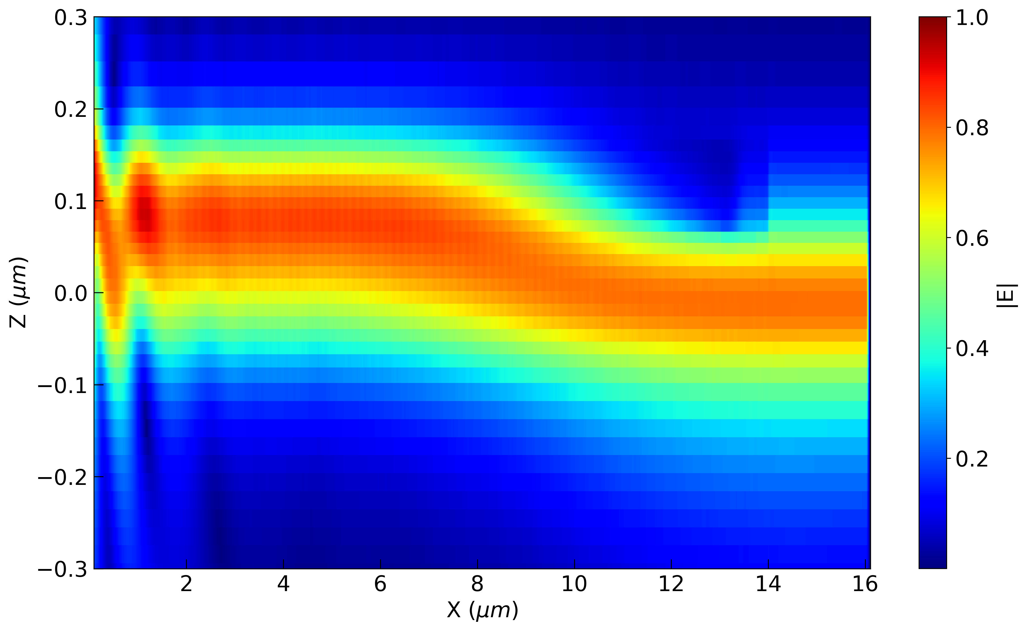
For a nanowaveguide with 9 um taper length, 17 nm/um taper slope, 120 nm thick waveguide and 100 nm thick nanowaveguide:
Coupling from emitter to nanowaveguide: 0.344
Coupling from nanowaveguide to waveguide: 0.974
Maximum total coupling from emitter to waveguide 0.335
Fabrication Robustness Simulation
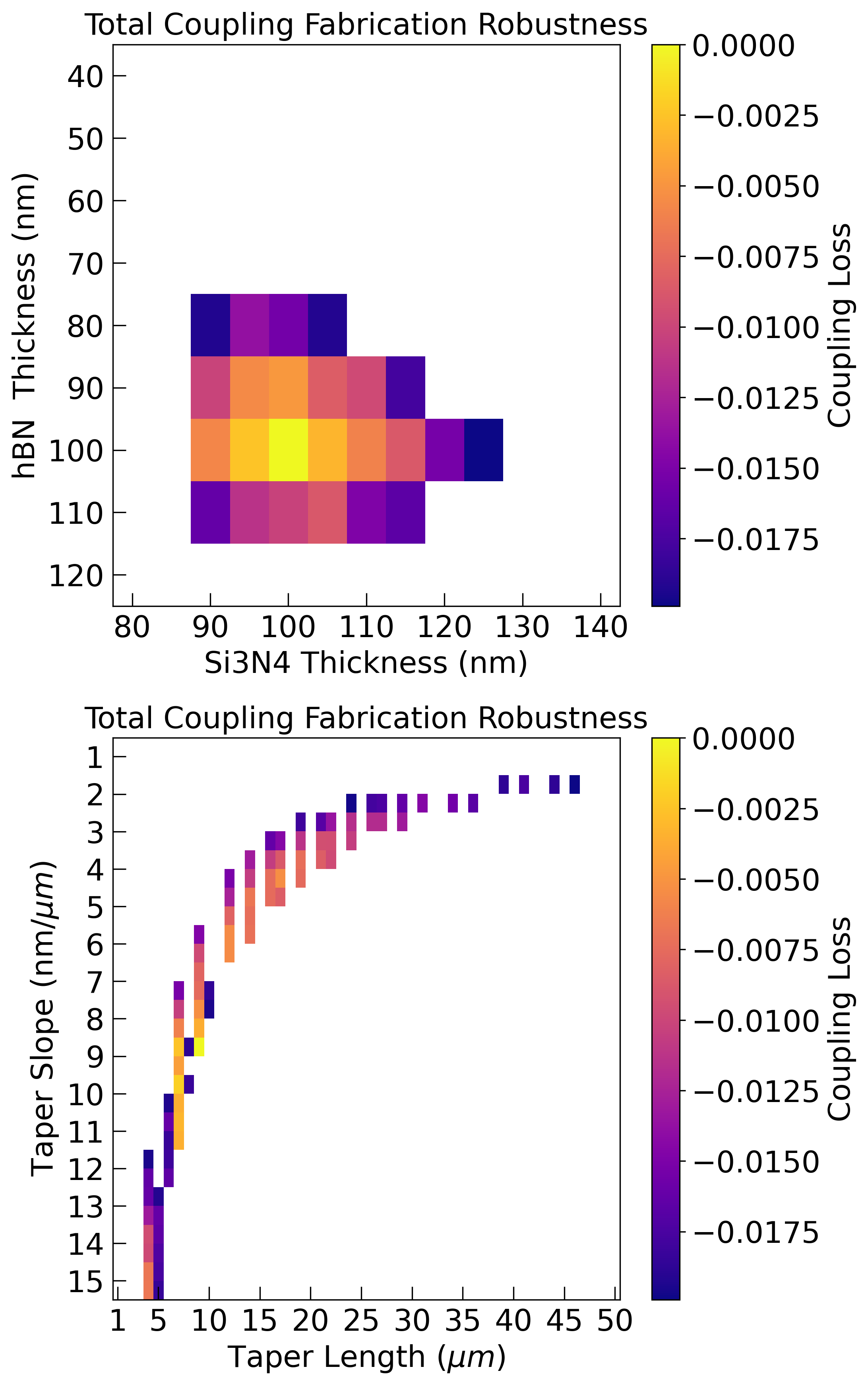
We have designed our optimized nanowaveguide. However, during fabrication, some parameters will differ from the design due to fabrication defects, so it is important to consider how robust our coupling is to deviations from our design. Based on our simulation sweeps, we already have the tools to see how deviations from our design will affect coupling. We do not know how deviations from the ideal emitter position and polarization will affect our coupling. First, we will replot our simulation sweep data in terms of coupling loss due to parameter deviation. Then, we will simulate our nanowaveguide with deviations in the emitter position and angle.
# Axes parameters
wg_tick = np.linspace(80, 140, 7)
nwg_tick = np.linspace(40, 120, 9)
len_tick = [1, 5, 10, 15, 20, 25, 30, 35, 40, 45, 50]
slope_tick = np.linspace(1e-3, 15e-3, 15) * 1e3

# Initialize figure
c_map = cm.get_cmap("plasma")
c_map.set_bad("white")
fig, axs = plt.subplots(2, 1)
fig.tight_layout()
fig.set_dpi(300)
fig.set_size_inches(6, 12)

# Find coupling loss with respect to ideal parameters
# try:
#     ideal_total_CE = ideal_total_CE.item()
# except:
#     None
max_wg_thick = np.max(np.max(Wg_mode_thick))
max_wg_tap = np.nanmax(np.nanmax(Wg_mode_tap))
Wg_mode_thick_fab = np.subtract(Wg_mode_thick, max_wg_thick)
Wg_mode_tap_fab = np.subtract(Wg_mode_tap, max_wg_tap)

Wg_mode_thick_fab[Wg_mode_thick_fab < -0.02] = np.nan
Wg_mode_tap_fab[Wg_mode_tap_fab < -0.02] = np.nan


# Plot and format
im1 = axs[0].imshow(
    Wg_mode_thick_fab,
    interpolation="none",
    cmap=c_map,
    aspect="auto",
    extent=[77.5, 142.5, 125, 35],
)
im2 = axs[1].imshow(
    Wg_mode_tap_fab,
    interpolation="none",
    cmap=c_map,
    aspect="auto",
    extent=[0.5, 50.5, 15.5, 0.5],
)

fig.set_size_inches(6, 12)
fig.set_dpi(300)

axs[0].set_title("Total Coupling Fabrication Robustness", fontsize=18)
axs[0].set_xlabel("Si3N4 Thickness (nm)", fontsize=18)
axs[0].set_ylabel("hBN  Thickness (nm)", fontsize=18)
axs[0].set_xticks(wg_tick)
axs[0].set_yticks(nwg_tick)
axs[0].tick_params(which="major", direction="in", length=8)
axs[0].tick_params(which="minor", direction="in", length=4)
axs[0].tick_params(axis="both", labelsize=18, pad=5)

axs[1].set_title("Total Coupling Fabrication Robustness", fontsize=18)
axs[1].set_ylabel("Taper Slope (nm/$\mu m$)", fontsize=18)
axs[1].set_xlabel("Taper Length ($\mu m$)", fontsize=18)
axs[1].set_xticks(len_tick)
axs[1].set_yticks(slope_tick)
axs[1].tick_params(which="major", direction="in", length=8)
axs[1].tick_params(which="minor", direction="in", length=4)
axs[1].tick_params(axis="both", labelsize=18, pad=5)

cbar1 = plt.colorbar(im1)
cbar1.set_label("Coupling Loss", fontsize=18)
cbar1.ax.tick_params(labelsize=18)

cbar2 = plt.colorbar(im2)
cbar2.set_label("Coupling Loss", fontsize=18)
cbar2.ax.tick_params(labelsize=18)

plt.show()
We define a simulation that lets the emitter position and polarization angle be varied.
def Nanowaveguide_sim_fab(dipole_height, dipole_dX, dipole_dY, polarization):

    # Set up simulation region size
    x_domain_size = (nwg_straight / 2 + taper_length + 2) * 2
    y_domain_size = 4 * waveguide_width
    z_domain_size = 1
    theta = polarization[0]
    phi = polarization[1]

    # Set up dipole source with variable polarization angles
    dipole = td.PointDipole.sources_from_angles(
        center=(dipole_dX, dipole_dY, waveguide_thickness / 2 + dipole_height),
        source_time=td.GaussianPulse(
            freq0=freq0,
            fwidth=fwidth,
        ),
        component="electric",
        angle_theta=theta,
        angle_phi=phi,
    )

    # Set up flux monitor for dipole power normalixation
    flux_dip = td.FluxMonitor(
        center=(0, 0, 0),
        size=(0.8 * x_domain_size, 0.8 * y_domain_size, 0.8 * z_domain_size),
        freqs=np.linspace(freq_beg, freq_end, 11),
        name="flux_dip",
    )

    # Set up mode monitor to measure power emitted into fundamental mode shared nanowaveguide and waveguide
    Nwg_mode = td.ModeMonitor(
        name="Nwg_mode",
        center=[(nwg_straight / 2) - 1, 0, 0],
        size=[0, td.inf, td.inf],
        freqs=np.linspace(freq_beg, freq_end, 11),
        mode_spec=td.ModeSpec(num_modes=1),
    )

    # Set up mode monitor to measure power coupled into fundamental waveguide mode
    Wg_mode = td.ModeMonitor(
        name="Wg_mode",
        center=[nwg_straight / 2 + taper_length + 1, 0, 0],
        size=[0, td.inf, td.inf],
        freqs=np.linspace(freq_beg, freq_end, 11),
        mode_spec=td.ModeSpec(num_modes=1),
    )

    # Set up waveguide structure
    Waveguide = td.Structure(
        name="Waveguide",
        geometry=td.Box(size=[td.inf, waveguide_width, waveguide_thickness]),
        medium=Si3N4,
    )

    # Set up substrate structure
    Substrate = td.Structure(
        geometry=td.Box(
            center=[0, 0, -sub_thickness / 2 - waveguide_thickness / 2],
            size=[td.inf, td.inf, sub_thickness],
        ),
        name="Substrate",
        medium=SiO2,
    )

    # Set up nanowaveguide structure. NOTE: If the taper length and slope are such that the nanowaveguide end in a single point, an error will occur.
    Nanowaveguide = td.Structure(
        geometry=td.PolySlab(
            slab_bounds=[
                waveguide_thickness / 2,
                waveguide_thickness / 2 + nwg_thickness,
            ],
            vertices=[
                [
                    -nwg_straight / 2 - taper_length,
                    nwg_width / 2 - taper_slope * taper_length,
                ],
                [-nwg_straight / 2, nwg_width / 2],
                [nwg_straight / 2, nwg_width / 2],
                [
                    nwg_straight / 2 + taper_length,
                    nwg_width / 2 - taper_slope * taper_length,
                ],
                [
                    nwg_straight / 2 + taper_length,
                    -(nwg_width / 2 - taper_slope * taper_length),
                ],
                [nwg_straight / 2, -nwg_width / 2],
                [-nwg_straight / 2, -nwg_width / 2],
                [
                    -nwg_straight / 2 - taper_length,
                    -(nwg_width / 2 - taper_slope * taper_length),
                ],
            ],
        ),
        name="Nanowaveguide",
        medium=hBN_ani,
    )

    # Create simulation
    min_steps_per_wvl = 6
    run_time = 1e-11
    shutoff = 5e-5

    sim = td.Simulation(
        size=[x_domain_size, y_domain_size, z_domain_size],
        center=(0, 0, 0),
        run_time=run_time,
        shutoff=shutoff,
        grid_spec=td.GridSpec.auto(
            min_steps_per_wvl=min_steps_per_wvl, wavelength=td.C_0 / freq0
        ),
        medium=vacuum,
        sources=[dipole[i] for i in range(len(dipole))],
        monitors=[Nwg_mode, Wg_mode, flux_dip],
        structures=[Waveguide, Substrate, Nanowaveguide],
    )

    return sim
# Start with dipole height simulation

# Define the sweep
dipole_height_sweep = np.arange(0.001, 0.1, 0.005)

# Define the path to save data
path = "data/20260126 dipole height sweep/"

# Build the simulation batch.
sims_dh = {
    f"dipole_height={dh * 1e3:.0f}nm": Nanowaveguide_sim_fab(
        dh, 0, 0, [np.pi / 2, np.pi / 2]
    )
    for dh in dipole_height_sweep
}
# Run the simulation batch
batch_dh = web.Batch(simulations=sims_dh)
est_fc = batch_dh.estimate_cost()
batch_dh_results = batch_dh.run(path_dir=path)
real_fc = batch_dh.real_cost()

# Next: deviation in emitter x position

# Define the sweep
dipole_dX_sweep = np.arange(0, 2, 0.1)

# Define the path to save data
path = "data/20260126 dipole X deviation sweep/"

# Build the simulation batch.
sims_dX = {
    f"dipole_dX={dX * 1e3:.0f}nm": Nanowaveguide_sim_fab(
        0, dX, 0, [np.pi / 2, np.pi / 2]
    )
    for dX in dipole_dX_sweep
}
# Run the simulation batch
batch_dX = web.Batch(simulations=sims_dX)
est_fc = batch_dX.estimate_cost()
batch_dX_results = batch_dX.run(path_dir=path)
real_fc = batch_dX.real_cost()

# Next: deviation in emitter y position

# Define the sweep
dipole_dY_sweep = np.arange(0, 0.199, 0.01)

# Define the path to save data
path = "data/20260126 dipole Y deviation sweep/"

# Build the simulation batch.
sims_dY = {
    f"dipole_dY={dY * 1e3:.0f}nm": Nanowaveguide_sim_fab(
        0, 0, dY, [np.pi / 2, np.pi / 2]
    )
    for dY in dipole_dY_sweep
}
# Run the simulation batch
batch_dY = web.Batch(simulations=sims_dY)
est_fc = batch_dY.estimate_cost()
batch_dY_results = batch_dY.run(path_dir=path)
real_fc = batch_dY.real_cost()


# Polarization Sweeps
dipole_theta_sweep = np.linspace(0, 1, 11) * np.pi / 2
path = "data/20260126 dipole theta sweep/"
sims_theta = {
    f"dipole_theta={t:.03}rad": Nanowaveguide_sim_fab(0, 0, 0, [t, np.pi / 2])
    for t in dipole_theta_sweep
}
batch_theta = web.Batch(simulations=sims_theta)
est_fc = batch_theta.estimate_cost()
batch_theta_results = batch_theta.run(path_dir=path)
real_fc = batch_theta.real_cost()


dipole_phi_sweep = np.linspace(0, 1, 11) * np.pi / 2
path = "data/20260126 dipole phi sweep/"
sims_phi = {
    f"dipole_phi={p:.03}rad": Nanowaveguide_sim_fab(0, 0, 0, [np.pi / 2, p])
    for p in dipole_phi_sweep
}
batch_phi = web.Batch(simulations=sims_phi)
est_fc = batch_phi.estimate_cost()
batch_phi_results = batch_phi.run(path_dir=path)
real_fc = batch_phi.real_cost()
13:04:57 -03 Maximum FlexCredit cost: 3.155 for the whole batch.
Output()
13:04:58 -03 Started working on Batch containing 20 tasks.
13:05:33 -03 Maximum FlexCredit cost: 3.155 for the whole batch.
             Use 'Batch.real_cost()' to get the billed FlexCredit cost after
             completion.
Output()
13:06:48 -03 Batch complete.
13:07:10 -03 Total billed flex credit cost: 0.662.
13:08:50 -03 Maximum FlexCredit cost: 3.155 for the whole batch.
Output()
13:08:52 -03 Started working on Batch containing 20 tasks.
13:09:25 -03 Maximum FlexCredit cost: 3.155 for the whole batch.
             Use 'Batch.real_cost()' to get the billed FlexCredit cost after
             completion.
Output()
13:11:31 -03 Batch complete.
13:11:51 -03 Total billed flex credit cost: 0.668.
13:13:32 -03 Maximum FlexCredit cost: 3.155 for the whole batch.
Output()
13:13:33 -03 Started working on Batch containing 20 tasks.
13:14:07 -03 Maximum FlexCredit cost: 3.155 for the whole batch.
             Use 'Batch.real_cost()' to get the billed FlexCredit cost after
             completion.
Output()
13:39:09 -03 Batch complete.
13:39:30 -03 Total billed flex credit cost: 0.662.
13:40:28 -03 Maximum FlexCredit cost: 1.735 for the whole batch.
Output()
13:40:29 -03 Started working on Batch containing 11 tasks.
13:40:48 -03 Maximum FlexCredit cost: 1.735 for the whole batch.
             Use 'Batch.real_cost()' to get the billed FlexCredit cost after
             completion.
Output()
13:43:33 -03 Batch complete.
13:43:44 -03 Total billed flex credit cost: 0.364.
13:44:40 -03 Maximum FlexCredit cost: 1.735 for the whole batch.
Output()
13:44:41 -03 Started working on Batch containing 11 tasks.
13:45:13 -03 Maximum FlexCredit cost: 1.735 for the whole batch.
             Use 'Batch.real_cost()' to get the billed FlexCredit cost after
             completion.
Output()
13:47:05 -03 Batch complete.
13:47:16 -03 Total billed flex credit cost: 0.364.
# Analyze the results
# Define arrays
Wg_mode_dh = np.zeros([len(dipole_height_sweep), 1])
Wg_mode_dX = np.zeros([len(dipole_dX_sweep), 1])
Wg_mode_dY = np.zeros([len(dipole_dY_sweep), 1])
Wg_mode_theta = np.zeros([len(dipole_theta_sweep), 1])
Wg_mode_phi = np.zeros([len(dipole_phi_sweep), 1])
# Populate data arrays with coupling coefficients averaged across simulated frequencies and normalized by the dipole source power
# Dipole height
for i in range(len(dipole_height_sweep)):
dh = dipole_height_sweep[i]
dipole_power = np.mean(
batch_dh_results[f"dipole_height={dh * 1e3:.0f}nm"]["flux_dip"].flux
)
norm_coup_wg = (
np.mean(
np.abs(
batch_dh_results[f"dipole_height={dh * 1e3:.0f}nm"]["Wg_mode"].amps.sel(
direction="+"
)
)
** 2
)
/ dipole_power
)
if i == 0:
max_dh = norm_coup_wg
Wg_mode_dh[i] = norm_coup_wg
Wg_mode_dh_loss = Wg_mode_dh - np.max(Wg_mode_dh)
# X Deviation
for i in range(len(dipole_dX_sweep)):
dX = dipole_dX_sweep[i]
dipole_power = np.mean(
batch_dX_results[f"dipole_dX={dX * 1e3:.0f}nm"]["flux_dip"].flux
)
norm_coup_wg = (
np.mean(
np.abs(
batch_dX_results[f"dipole_dX={dX * 1e3:.0f}nm"]["Wg_mode"].amps.sel(
direction="+"
)
)
** 2
)
/ dipole_power
)
Wg_mode_dX[i] = norm_coup_wg
Wg_mode_dX_loss = Wg_mode_dX - Wg_mode_dX[0]
# Y Deviation
for i in range(len(dipole_dY_sweep)):
dY = dipole_dY_sweep[i]
dipole_power = np.mean(
batch_dY_results[f"dipole_dY={dY * 1e3:.0f}nm"]["flux_dip"].flux
)
norm_coup_wg = (
np.mean(
np.abs(
batch_dY_results[f"dipole_dY={dY * 1e3:.0f}nm"]["Wg_mode"].amps.sel(
direction="+"
)
)
** 2
)
/ dipole_power
)
Wg_mode_dY[i] = norm_coup_wg
Wg_mode_dY_loss = Wg_mode_dY - Wg_mode_dY[0]
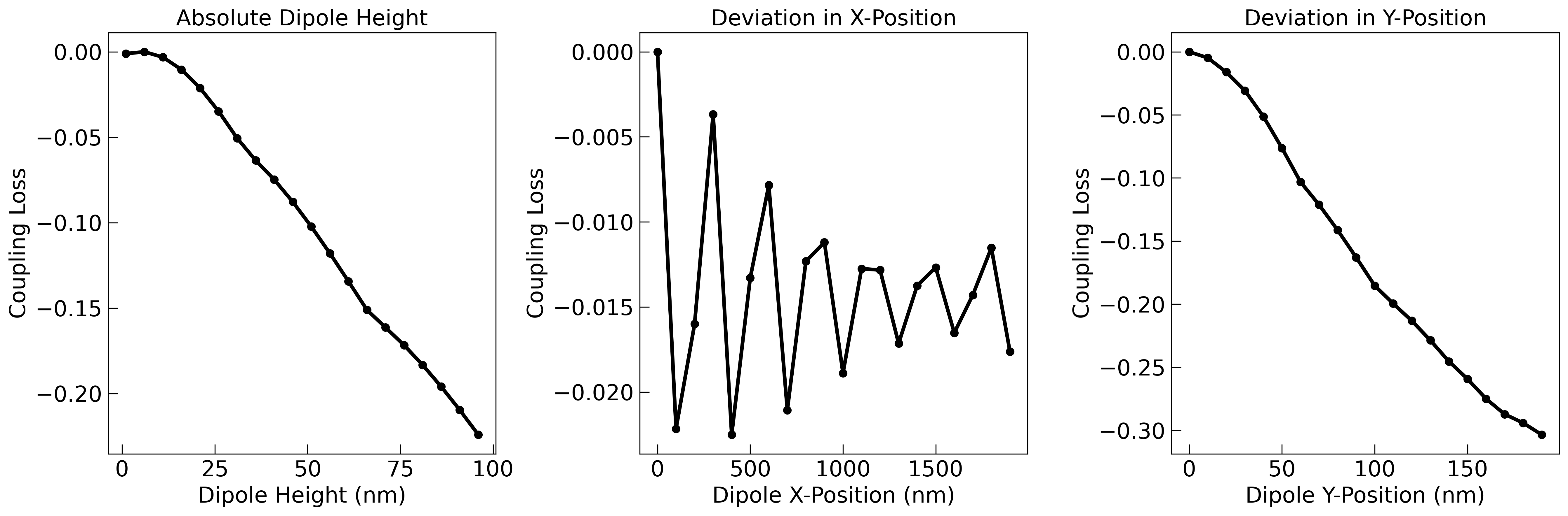
# Plot coupling loss as a function of emitter position deviation
fig1, ax = plt.subplots(1, 3)
fig1.set_size_inches(18, 6)
fig1.tight_layout()
fig1.set_dpi(300)
ax[0].plot(dipole_height_sweep * 1e3, Wg_mode_dh_loss, color="black", linewidth=3)
ax[1].plot(dipole_dX_sweep * 1e3, Wg_mode_dX_loss, color="black", linewidth=3)
ax[2].plot(dipole_dY_sweep * 1e3, Wg_mode_dY_loss, color="black", linewidth=3)
ax[0].scatter(dipole_height_sweep * 1e3, Wg_mode_dh_loss, color="black")
ax[1].scatter(dipole_dX_sweep * 1e3, Wg_mode_dX_loss, color="black")
ax[2].scatter(dipole_dY_sweep * 1e3, Wg_mode_dY_loss, color="black")
ax[0].set_title("Absolute Dipole Height", fontsize=18)
ax[0].set_ylabel("Coupling Loss", fontsize=18)
ax[0].set_xlabel("Dipole Height (nm)", fontsize=18)
ax[0].tick_params(which="major", direction="in", length=8)
ax[0].tick_params(which="minor", direction="in", length=4)
ax[0].tick_params(axis="both", labelsize=18, pad=5)
ax[1].set_title("Deviation in X-Position", fontsize=18)
ax[1].set_ylabel("Coupling Loss", fontsize=18)
ax[1].set_xlabel("Dipole X-Position (nm)", fontsize=18)
ax[1].tick_params(which="major", direction="in", length=8)
ax[1].tick_params(which="minor", direction="in", length=4)
ax[1].tick_params(axis="both", labelsize=18, pad=5)
ax[2].set_title("Deviation in Y-Position", fontsize=18)
ax[2].set_ylabel("Coupling Loss", fontsize=18)
ax[2].set_xlabel("Dipole Y-Position (nm)", fontsize=18)
ax[2].tick_params(which="major", direction="in", length=8)
ax[2].tick_params(which="minor", direction="in", length=4)
ax[2].tick_params(axis="both", labelsize=18, pad=5)
fig1.tight_layout()
plt.show()
# Plot coupling loss as a function of emitter polarization
# Theta
for i in range(len(dipole_theta_sweep)):
t = dipole_theta_sweep[i]
dipole_power = np.mean(
batch_theta_results[f"dipole_theta={t:.03}rad"]["flux_dip"].flux
)
norm_coup_wg = (
np.mean(
np.abs(
batch_theta_results[f"dipole_theta={t:.03}rad"]["Wg_mode"].amps.sel(
direction="+"
)
)
** 2
)
/ dipole_power
)
Wg_mode_theta[i] = norm_coup_wg
Wg_mode_theta_loss = Wg_mode_theta - Wg_mode_theta[-1]
# Phi
for i in range(len(dipole_phi_sweep)):
p = dipole_phi_sweep[i]
dipole_power = np.mean(batch_phi_results[f"dipole_phi={p:.03}rad"]["flux_dip"].flux)
norm_coup_wg = (
np.mean(
np.abs(
batch_phi_results[f"dipole_phi={p:.03}rad"]["Wg_mode"].amps.sel(
direction="+"
)
)
** 2
)
/ dipole_power
)
Wg_mode_phi[i] = norm_coup_wg - ideal_total_CE
Wg_mode_phi_loss = Wg_mode_phi - Wg_mode_phi[-1]
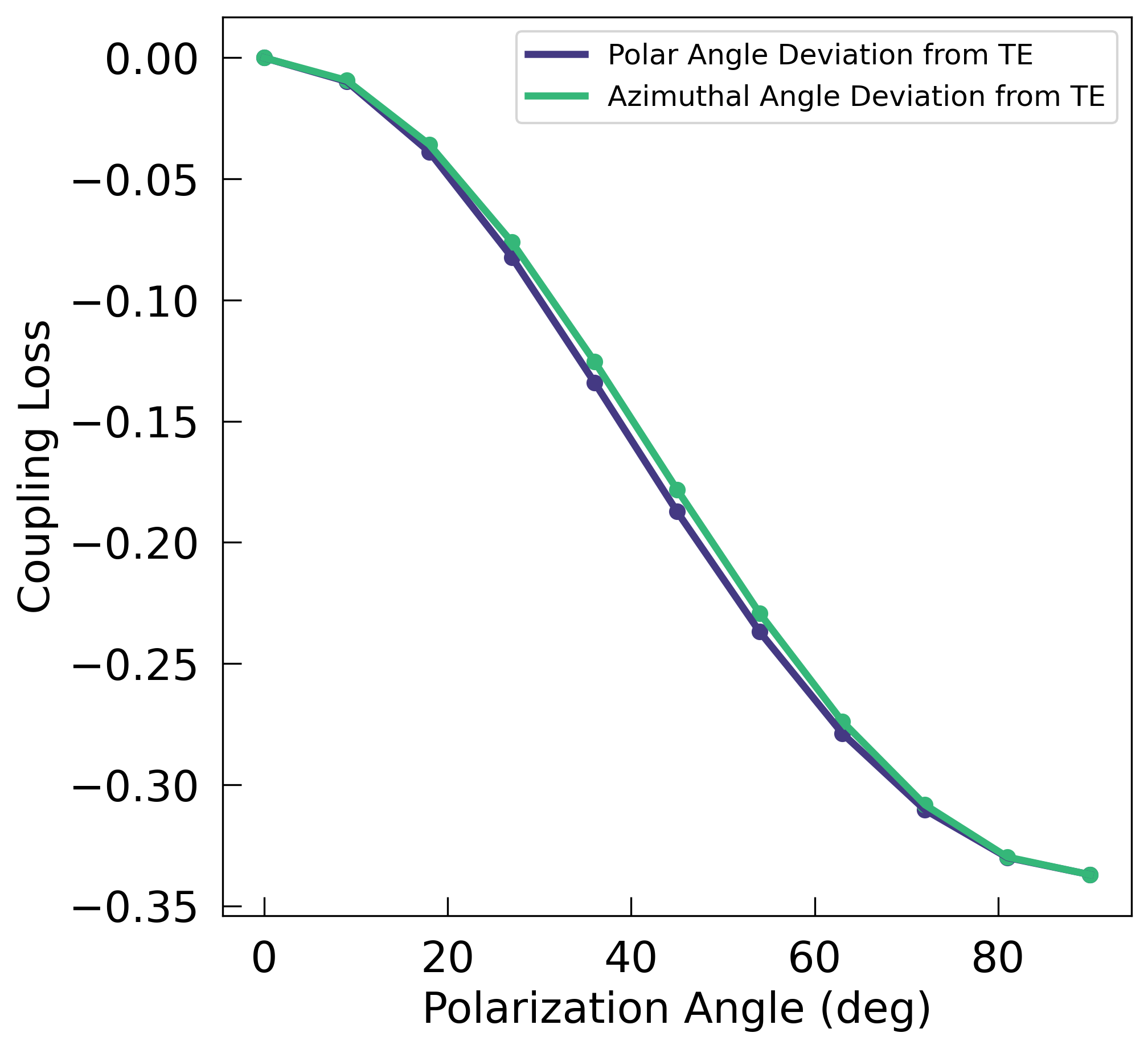
fig2, axs = plt.subplots()
cmap = mpl.colormaps["viridis"]
colors = cmap(np.linspace(0, 1, 7))
fig2.tight_layout()
fig2.set_dpi(300)
fig2.set_size_inches(6, 6)
axs.plot(
90 - dipole_theta_sweep * 180 / np.pi,
Wg_mode_theta_loss,
color=colors[1],
label="Polar Angle Deviation from TE",
linewidth=3,
)
axs.scatter(90 - dipole_theta_sweep * 180 / np.pi, Wg_mode_theta_loss, color=colors[1])
axs.plot(
90 - dipole_phi_sweep * 180 / np.pi,
Wg_mode_phi_loss,
color=colors[4],
label="Azimuthal Angle Deviation from TE",
linewidth=3,
)
axs.scatter(90 - dipole_phi_sweep * 180 / np.pi, Wg_mode_phi_loss, color=colors[4])
axs.set_xlabel("Polarization Angle (deg)", fontsize=18)
axs.set_ylabel("Coupling Loss", fontsize=18)
axs.legend(loc="upper right", fontsize=12)
axs.tick_params(which="major", direction="in", length=8)
axs.tick_params(which="minor", direction="in", length=4)
axs.tick_params(axis="both", labelsize=18, pad=10)
plt.show()
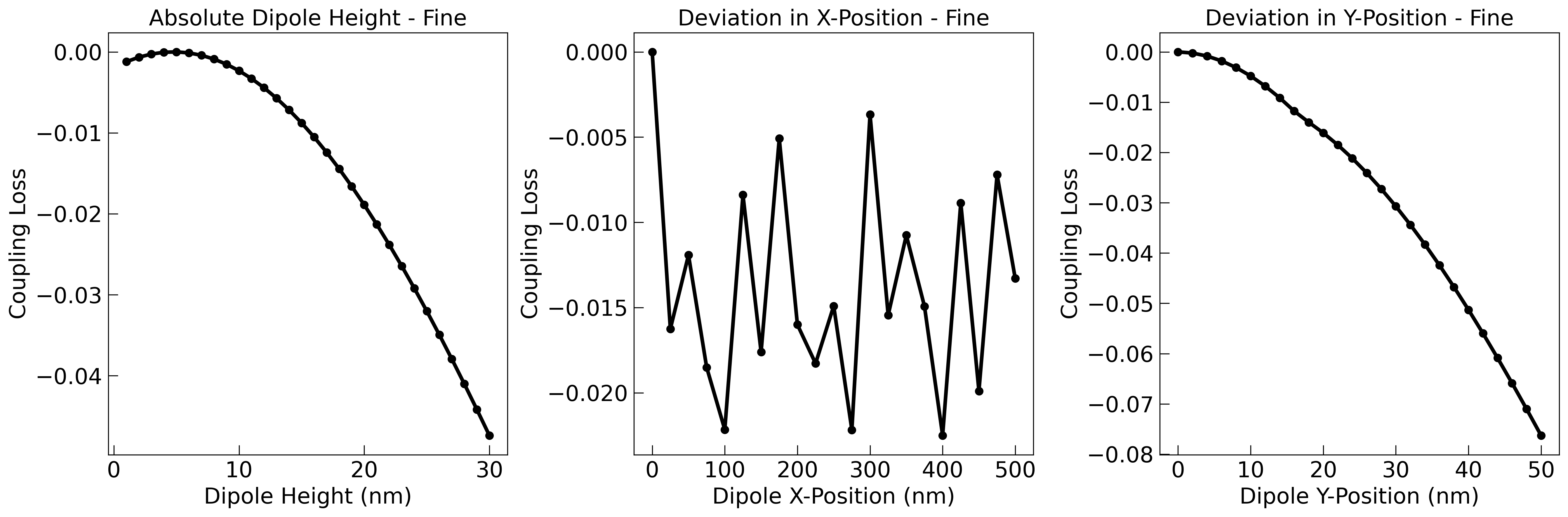
We refine the robustness sweep around the regime with coupling loss of roughly -5% or less.
# Same simulation order as before

# Define finer the sweep for dipole height up to
dipole_height_sweep_fine = np.arange(0.001, 0.031, 0.001)

# Define the path to save data
path = "data/20260126 dipole height sweep fine/"

# Build the simulation batch. We include an if statement to filter out invalid cases where the taper length is too long for larger taper slopes resulting in invalid polygons.
sims_dh_fine = {
    f"dipole_height={dh * 1e3:.0f}nm": Nanowaveguide_sim_fab(
        dh, 0, 0, [np.pi / 2, np.pi / 2]
    )
    for dh in dipole_height_sweep_fine
}
# Run the simulation batch
batch_dh_fine = web.Batch(simulations=sims_dh_fine)
est_fc = batch_dh_fine.estimate_cost()
batch_dh_fine_results = batch_dh_fine.run(path_dir=path)
real_fc = batch_dh_fine.real_cost()


# None of the X-position deviations showed larger coupling losses. Let's decrease the step size to see if there is a smoother couplign dependence on X-position.

# Define the sweep
dipole_dX_sweep_fine = np.arange(0, 0.525, 0.025)

# Define the path to save data
path = "data/20260126 dipole X deviation sweep fine/"

# Build the simulation batch. We include an if statement to filter out invalid cases where the taper length is too long for larger taper slopes resulting in invalid polygons.
sims_dX_fine = {
    f"dipole_dX={dX * 1e3:.0f}nm": Nanowaveguide_sim_fab(
        0, dX, 0, [np.pi / 2, np.pi / 2]
    )
    for dX in dipole_dX_sweep_fine
}
# Run the simulation batch
batch_dX_fine = web.Batch(simulations=sims_dX_fine)
est_fc = batch_dX_fine.estimate_cost()
batch_dX_fine_results = batch_dX_fine.run(path_dir=path)
real_fc = batch_dX_fine.real_cost()

# Next: deviation in emitter y position

# Define the sweep
dipole_dY_sweep_fine = np.arange(0, 0.052, 0.002)

# Define the path to save data
path = "data/20260126 dipole Y deviation sweep fine/"

# Build the simulation batch. We include an if statement to filter out invalid cases where the taper length is too long for larger taper slopes resulting in invalid polygons.
sims_dY_fine = {
    f"dipole_dY={dY * 1e3:.0f}nm": Nanowaveguide_sim_fab(
        0, 0, dY, [np.pi / 2, np.pi / 2]
    )
    for dY in dipole_dY_sweep_fine
}
# Run the simulation batch
batch_dY_fine = web.Batch(simulations=sims_dY_fine)
est_fc = batch_dY_fine.estimate_cost()
batch_dY_fine_results = batch_dY_fine.run(path_dir=path)
real_fc = batch_dY_fine.real_cost()


# Polarization Sweeps
dipole_theta_sweep_fine = np.linspace(0.8, 1, 11) * np.pi / 2
path = "data/20260126 dipole theta sweep fine/"
sims_theta_fine = {
    f"dipole_theta={t:.03}rad": Nanowaveguide_sim_fab(0, 0, 0, [t, np.pi / 2])
    for t in dipole_theta_sweep_fine
}
batch_theta_fine = web.Batch(simulations=sims_theta_fine)
est_fc = batch_theta_fine.estimate_cost()
batch_theta_fine_results = batch_theta_fine.run(path_dir=path)
real_fc = batch_theta_fine.real_cost()


dipole_phi_sweep_fine = np.linspace(0.8, 1, 11) * np.pi / 2
path = "data/20260114 dipole phi sweep fine/"
sims_phi_fine = {
    f"dipole_phi={p:.03}rad": Nanowaveguide_sim_fab(0, 0, 0, [np.pi / 2, p])
    for p in dipole_phi_sweep_fine
}
batch_phi_fine = web.Batch(simulations=sims_phi_fine)
est_fc = batch_phi_fine.estimate_cost()
batch_phi_fine_results = batch_phi_fine.run(path_dir=path)
real_fc = batch_phi_fine.real_cost()
13:52:06 -03 Maximum FlexCredit cost: 4.732 for the whole batch.
Output()
13:52:09 -03 Started working on Batch containing 30 tasks.
13:53:01 -03 Maximum FlexCredit cost: 4.732 for the whole batch.
             Use 'Batch.real_cost()' to get the billed FlexCredit cost after
             completion.
Output()
13:55:03 -03 Batch complete.
13:55:35 -03 Total billed flex credit cost: 0.993.
13:57:25 -03 Maximum FlexCredit cost: 3.312 for the whole batch.
Output()
13:57:27 -03 Started working on Batch containing 21 tasks.
13:58:24 -03 Maximum FlexCredit cost: 3.312 for the whole batch.
             Use 'Batch.real_cost()' to get the billed FlexCredit cost after
             completion.
Output()
13:59:19 -03 Batch complete.
13:59:41 -03 Total billed flex credit cost: 0.695.
14:02:09 -03 Maximum FlexCredit cost: 4.101 for the whole batch.
Output()
14:02:10 -03 Started working on Batch containing 26 tasks.
14:02:57 -03 Maximum FlexCredit cost: 4.101 for the whole batch.
             Use 'Batch.real_cost()' to get the billed FlexCredit cost after
             completion.
Output()
14:05:41 -03 Batch complete.
14:06:07 -03 Total billed flex credit cost: 0.861.
14:07:04 -03 Maximum FlexCredit cost: 1.735 for the whole batch.
Output()
Started working on Batch containing 11 tasks.
14:07:24 -03 Maximum FlexCredit cost: 1.735 for the whole batch.
             Use 'Batch.real_cost()' to get the billed FlexCredit cost after
             completion.
Output()
14:08:04 -03 Batch complete.
14:08:15 -03 Total billed flex credit cost: 0.364.
14:09:11 -03 Maximum FlexCredit cost: 1.735 for the whole batch.
Output()
14:09:12 -03 Started working on Batch containing 11 tasks.
14:09:32 -03 Maximum FlexCredit cost: 1.735 for the whole batch.
             Use 'Batch.real_cost()' to get the billed FlexCredit cost after
             completion.
Output()
14:14:49 -03 Batch complete.
14:15:01 -03 Total billed flex credit cost: 0.364.
# Analyze the fine sweep results
# Define arrays
Wg_mode_dh_fine = np.zeros([len(dipole_height_sweep_fine), 1])
Wg_mode_dX_fine = np.zeros([len(dipole_dX_sweep_fine), 1])
Wg_mode_dY_fine = np.zeros([len(dipole_dY_sweep_fine), 1])
Wg_mode_theta_fine = np.zeros([len(dipole_theta_sweep_fine), 1])
Wg_mode_phi_fine = np.zeros([len(dipole_phi_sweep_fine), 1])
# Populate data arrays with coupling coefficients averaged across simulated frequencies and normalized by the dipole source power
# Dipole height
for i in range(len(dipole_height_sweep_fine)):
dh = dipole_height_sweep_fine[i]
dipole_power = np.mean(
batch_dh_fine_results[f"dipole_height={dh * 1e3:.0f}nm"]["flux_dip"].flux
)
norm_coup_wg = (
np.mean(
np.abs(
batch_dh_fine_results[f"dipole_height={dh * 1e3:.0f}nm"][
"Wg_mode"
].amps.sel(direction="+")
)
** 2
)
/ dipole_power
)
if i == 0:
max_dh = norm_coup_wg
Wg_mode_dh_fine[i] = norm_coup_wg
Wg_mode_dh_fine_loss = Wg_mode_dh_fine - np.max(Wg_mode_dh_fine)
# X Deviation
for i in range(len(dipole_dX_sweep_fine)):
dX = dipole_dX_sweep_fine[i]
dipole_power = np.mean(
batch_dX_fine_results[f"dipole_dX={dX * 1e3:.0f}nm"]["flux_dip"].flux
)
norm_coup_wg = (
np.mean(
np.abs(
batch_dX_fine_results[f"dipole_dX={dX * 1e3:.0f}nm"][
"Wg_mode"
].amps.sel(direction="+")
)
** 2
)
/ dipole_power
)
Wg_mode_dX_fine[i] = norm_coup_wg
Wg_mode_dX_fine_loss = Wg_mode_dX_fine - Wg_mode_dX_fine[0]
# Y Deviation
for i in range(len(dipole_dY_sweep_fine)):
dY = dipole_dY_sweep_fine[i]
dipole_power = np.mean(
batch_dY_fine_results[f"dipole_dY={dY * 1e3:.0f}nm"]["flux_dip"].flux
)
norm_coup_wg = (
np.mean(
np.abs(
batch_dY_fine_results[f"dipole_dY={dY * 1e3:.0f}nm"][
"Wg_mode"
].amps.sel(direction="+")
)
** 2
)
/ dipole_power
)
Wg_mode_dY_fine[i] = norm_coup_wg
Wg_mode_dY_fine_loss = Wg_mode_dY_fine - Wg_mode_dY_fine[0]
# Plot coupling loss as a function of emitter position deviation
fig1, ax = plt.subplots(1, 3)
fig1.set_size_inches(18, 6)
fig1.tight_layout()
fig1.set_dpi(300)
ax[0].plot(
dipole_height_sweep_fine * 1e3, Wg_mode_dh_fine_loss, color="black", linewidth=3
)
ax[1].plot(dipole_dX_sweep_fine * 1e3, Wg_mode_dX_fine_loss, color="black", linewidth=3)
ax[2].plot(dipole_dY_sweep_fine * 1e3, Wg_mode_dY_fine_loss, color="black", linewidth=3)
ax[0].scatter(dipole_height_sweep_fine * 1e3, Wg_mode_dh_fine_loss, color="black")
ax[1].scatter(dipole_dX_sweep_fine * 1e3, Wg_mode_dX_fine_loss, color="black")
ax[2].scatter(dipole_dY_sweep_fine * 1e3, Wg_mode_dY_fine_loss, color="black")
ax[0].set_title("Absolute Dipole Height - Fine", fontsize=18)
ax[0].set_ylabel("Coupling Loss", fontsize=18)
ax[0].set_xlabel("Dipole Height (nm)", fontsize=18)
ax[0].tick_params(which="major", direction="in", length=8)
ax[0].tick_params(which="minor", direction="in", length=4)
ax[0].tick_params(axis="both", labelsize=18, pad=5)
ax[1].set_title("Deviation in X-Position - Fine", fontsize=18)
ax[1].set_ylabel("Coupling Loss", fontsize=18)
ax[1].set_xlabel("Dipole X-Position (nm)", fontsize=18)
ax[1].tick_params(which="major", direction="in", length=8)
ax[1].tick_params(which="minor", direction="in", length=4)
ax[1].tick_params(axis="both", labelsize=18, pad=5)
ax[2].set_title("Deviation in Y-Position - Fine", fontsize=18)
ax[2].set_ylabel("Coupling Loss", fontsize=18)
ax[2].set_xlabel("Dipole Y-Position (nm)", fontsize=18)
ax[2].tick_params(which="major", direction="in", length=8)
ax[2].tick_params(which="minor", direction="in", length=4)
ax[2].tick_params(axis="both", labelsize=18, pad=5)
fig1.tight_layout()
plt.show()
# Plot coupling loss as a function of emitter polarization
# Theta
for i in range(len(dipole_theta_sweep_fine)):
t = dipole_theta_sweep_fine[i]
dipole_power = np.mean(
batch_theta_fine_results[f"dipole_theta={t:.03}rad"]["flux_dip"].flux
)
norm_coup_wg = (
np.mean(
np.abs(
batch_theta_fine_results[f"dipole_theta={t:.03}rad"][
"Wg_mode"
].amps.sel(direction="+")
)
** 2
)
/ dipole_power
)
Wg_mode_theta_fine[i] = norm_coup_wg
Wg_mode_theta_fine_loss = Wg_mode_theta_fine - Wg_mode_theta_fine[-1]
# Phi
for i in range(len(dipole_phi_sweep_fine)):
p = dipole_phi_sweep_fine[i]
dipole_power = np.mean(
batch_phi_fine_results[f"dipole_phi={p:.03}rad"]["flux_dip"].flux
)
norm_coup_wg = (
np.mean(
np.abs(
batch_phi_fine_results[f"dipole_phi={p:.03}rad"]["Wg_mode"].amps.sel(
direction="+"
)
)
** 2
)
/ dipole_power
)
Wg_mode_phi_fine[i] = norm_coup_wg
Wg_mode_phi_fine_loss = Wg_mode_phi_fine - Wg_mode_phi_fine[-1]
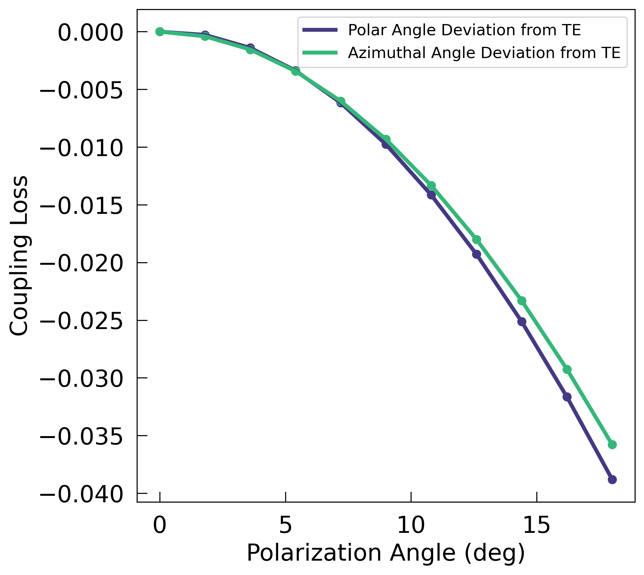
fig2, axs = plt.subplots()
cmap = mpl.colormaps["viridis"]
colors = cmap(np.linspace(0, 1, 7))
fig2.tight_layout()
fig2.set_dpi(300)
fig2.set_size_inches(6, 6)
axs.plot(
90 - dipole_theta_sweep_fine * 180 / np.pi,
Wg_mode_theta_fine_loss,
color=colors[1],
label="Polar Angle Deviation from TE",
linewidth=3,
)
axs.scatter(
90 - dipole_theta_sweep_fine * 180 / np.pi, Wg_mode_theta_fine_loss, color=colors[1]
)
axs.plot(
90 - dipole_phi_sweep_fine * 180 / np.pi,
Wg_mode_phi_fine_loss,
color=colors[4],
label="Azimuthal Angle Deviation from TE",
linewidth=3,
)
axs.scatter(
90 - dipole_phi_sweep_fine * 180 / np.pi, Wg_mode_phi_fine_loss, color=colors[4]
)
axs.set_xlabel("Polarization Angle (deg)", fontsize=18)
axs.set_ylabel("Coupling Loss", fontsize=18)
axs.legend(loc="upper right", fontsize=12)
axs.tick_params(which="major", direction="in", length=8)
axs.tick_params(which="minor", direction="in", length=4)
axs.tick_params(axis="both", labelsize=18, pad=10)
plt.show()
NbTiN SNSPD Simulation
We now turn to the integration and coupling of our second heterogeneous material: NbTiN nanowires used for the detection of single photons.
First, we define parameters that will remain constant for the SNSPD simulations. The NbTiN complex refractive index is modeled as an (n, k) material with the values for n and k at 585 nm taken from Banerjee, A. et al. Optical properties of refractory metal based thin films. Opt. Mat. Express 8 (8), 2072-2088 (2018). DOI: 10.1364/OME.8.002072.
# Wavelength
lda0 = 0.585
freq0 = td.C_0 / lda0

# Geometrical Parameters
waveguide_width = 0.4
waveguide_thickness = 0.12
nanowire_thickness = 0.0076

# Set up simulation region size
x_domain_size = 0
y_domain_size = 4 * waveguide_width
z_domain_size = 1

# Materials
NbTiN = td.Lorentz.from_nk(
    name="NbTiN", n=2.2, k=2.24, freq=freq0
)  # NbTiN n,k value at 585nm
SiO2 = td.material_library["SiO2"]["Horiba"]
Si3N4 = td.material_library["Si3N4"]["Philipp1973Sellmeier"]

box = td.Box.from_bounds(
    rmin=(-10, -1, -0.1),
    rmax=(10, 1, 0.1),
)
Now, we create the SNSPD simulation. Unlike the hBN nanowaveguide, we can sweep our parameters using only the mode solver, because SNSPD coupling is directly proportional to the imaginary effective refractive index of the waveguide mode.
def mode_solver(nanowire_width, gap):
    # Structures
    Substrate = td.Structure(
        geometry=td.Box.from_bounds(
            rmin=(-td.inf, -td.inf, -2 * z_domain_size), rmax=(td.inf, td.inf, 0)
        ),
        name="Substrate",
        medium=SiO2,
    )

    Waveguide = td.Structure(
        geometry=td.Box(
            center=[0, 0, waveguide_thickness / 2],
            size=[td.inf, waveguide_width, waveguide_thickness],
        ),
        name="Waveguide",
        medium=Si3N4,
    )

    Nanowire_1 = td.Structure(
        geometry=td.Box(
            center=[
                0,
                -(nanowire_width + gap) / 2,
                waveguide_thickness + nanowire_thickness / 2,
            ],
            size=[td.inf, nanowire_width, nanowire_thickness],
        ),
        name="nanowire_1",
        medium=NbTiN,
    )

    Nanowire_2 = td.Structure(
        geometry=td.Box(
            center=[
                0,
                (nanowire_width + gap) / 2,
                waveguide_thickness + nanowire_thickness / 2,
            ],
            size=[td.inf, nanowire_width, nanowire_thickness],
        ),
        name="nanowire2",
        medium=NbTiN,
    )

    # Mesh
    refine_box1 = td.MeshOverrideStructure(
        geometry=td.Box(
            center=[
                0,
                -(nanowire_width + gap) / 2,
                waveguide_thickness + nanowire_thickness / 2,
            ],
            size=[0, nanowire_width, nanowire_thickness],
        ),
        dl=[None, 0.005, 0.001],
    )  # refined mesh for Nanowire_1

    refine_box2 = td.MeshOverrideStructure(
        geometry=td.Box(
            center=[
                0,
                (nanowire_width + gap) / 2,
                waveguide_thickness + nanowire_thickness / 2,
            ],
            size=[0, nanowire_width, nanowire_thickness],
        ),
        dl=[None, 0.005, 0.001],
    )  # refined mesh for Nanowire_2

    sim = td.Simulation(
        center=(0, 0, 0),
        size=(x_domain_size, y_domain_size, z_domain_size),
        grid_spec=td.GridSpec.auto(
            wavelength=0.585,
            min_steps_per_wvl=30,
            override_structures=[refine_box1, refine_box2],
        ),
        boundary_spec=td.BoundarySpec(
            x=td.Boundary.periodic(), z=td.Boundary.pml(), y=td.Boundary.pml()
        ),
        structures=[Substrate, Waveguide, Nanowire_1, Nanowire_2],
        run_time=1e-12,
    )

    mode_spec = td.ModeSpec(num_modes=1, target_neff=2)

    mode_solver = ModeSolver(
        simulation=sim,
        plane=td.Box(
            center=(0, 0, 0), size=(x_domain_size, y_domain_size, z_domain_size)
        ),
        mode_spec=mode_spec,
        freqs=[freq0],
    )

    return mode_solver
We run a parameter sweep over the nanowire width and the gap between nanowires.
nanowire_width_list = np.linspace(0.05, 0.15, 11)
gap_list = np.linspace(0.05, 0.15, 11)

mode_solvers = {
    f"nanowire_width={nanowire_width:.3f};gap={gap:.3f}": mode_solver(
        nanowire_width, gap
    )
    for nanowire_width in nanowire_width_list
    for gap in gap_list
    if 2 * nanowire_width + gap < waveguide_width
}

batch_SNSPD = web.Batch(simulations=mode_solvers)
batch_SNSPD_results = batch_SNSPD.run(
    path_dir="data/20260127 SNSPD gap and nw width sweep/"
)
real_fc = batch_SNSPD.real_cost()
Output()
14:18:39 -03 Started working on Batch containing 111 tasks.
14:21:42 -03 Maximum FlexCredit cost: 0.427 for the whole batch.
             Use 'Batch.real_cost()' to get the billed FlexCredit cost after
             completion.
Output()
14:36:11 -03 Batch complete.
14:39:31 -03 Total billed flex credit cost: 0.427.
We then compute the coupling based on the imaginary part of the waveguide mode effective index.
loss = np.array(
    [
        [
            (
                4.34
                * 1e-6
                * 4
                * np.pi
                * batch_SNSPD_results[
                    f"nanowire_width={nanowire_width:.3f};gap={gap:.3f}"
                ]
                .k_eff.sel(f=freq0)
                .values.item()
                / (lda0 * 1e-6)
            )
            if (2 * nanowire_width + gap < waveguide_width)
            else np.nan
            for gap in gap_list
        ]
        for nanowire_width in nanowire_width_list
    ],
    dtype=float,
)


widths_tick = np.linspace(50, 150, 11)  # nanowire width (nm)
gaps_tick = np.linspace(50, 150, 6)  # gap (nm)

c_map = cm.get_cmap("plasma").copy()
c_map.set_bad("white")

loss_copy = loss.copy()
loss[loss == 0] = np.nan  # remove if 0 is a valid value

# Initialize figure
fig, ax = plt.subplots(1, 1)
fig.tight_layout()

# Half-step padding so pixels align with ticks
step = widths_tick[1] - widths_tick[0]

extent = [
    widths_tick[0] - step / 2,
    widths_tick[-1] + step / 2,
    gaps_tick[-1] + step / 2,
    gaps_tick[0] - step / 2,
]

im = ax.imshow(loss, interpolation="none", cmap=c_map, aspect="auto", extent=extent)

fig.set_size_inches(6, 6)
fig.set_dpi(300)

ax.set_title("Absorption", fontsize=18)
ax.set_xlabel("Gap (nm)", fontsize=18)
ax.set_ylabel("Nanowire Width (nm)", fontsize=18)

ax.set_yticks(widths_tick)
ax.set_xticks(gaps_tick)

ax.tick_params(which="major", direction="in", length=8)
ax.tick_params(which="minor", direction="in", length=4)
ax.tick_params(axis="both", labelsize=18, pad=5)

cbar = plt.colorbar(im, ax=ax)
cbar.set_label("Absorption (dB/$\\mu$m)", fontsize=18)
cbar.ax.tick_params(labelsize=18)

plt.show()
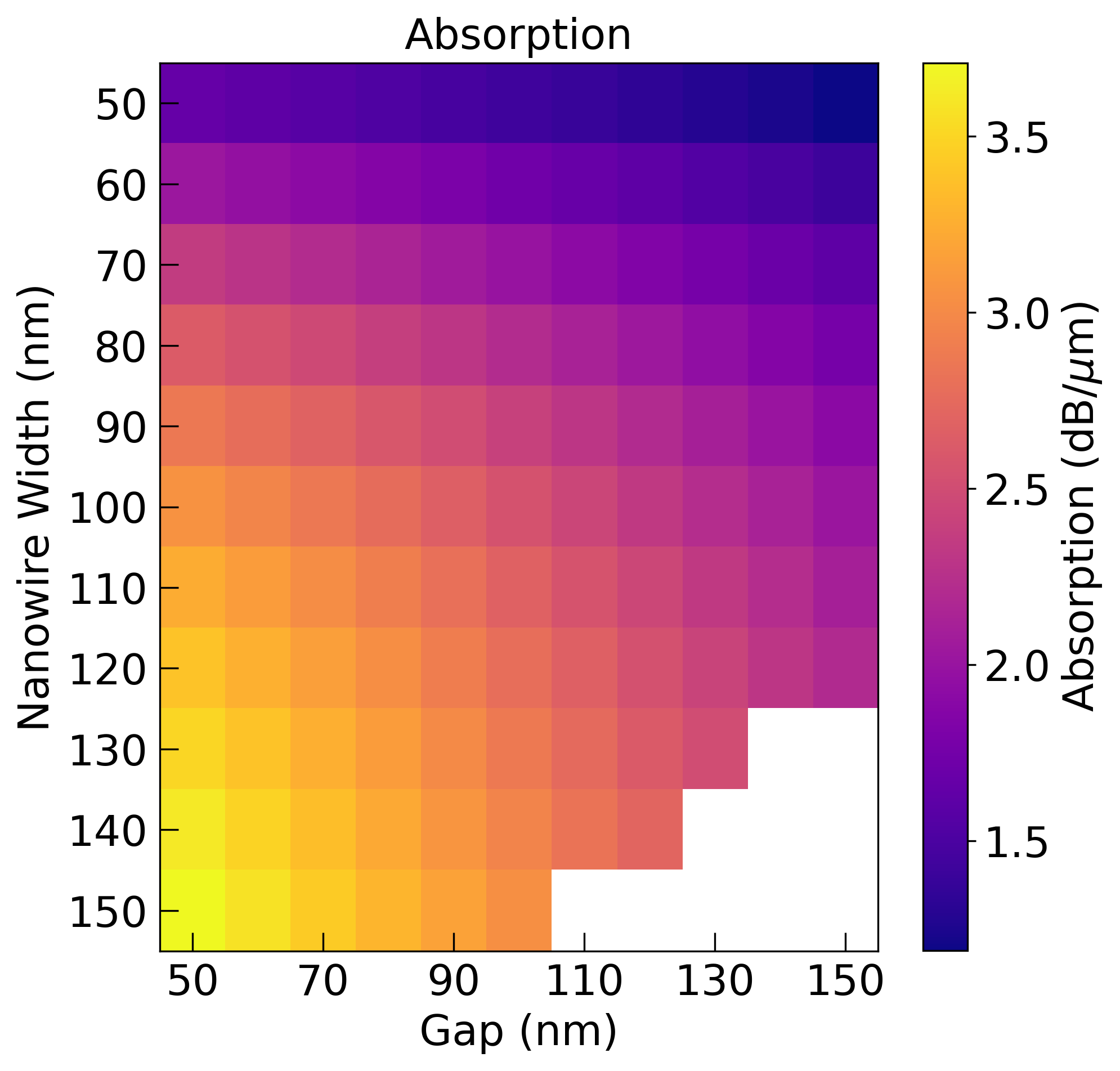
max_flat_index = np.nanargmax(loss)
width_ind, gap_ind = np.unravel_index(max_flat_index, loss.shape)

max_gap = gap_list[gap_ind]
max_width = nanowire_width_list[width_ind]
max_coup = loss[width_ind][gap_ind]

print(
    f"Maximum total coupling of {max_coup:.3f} dB/um with {max_gap * 1e3:.1f} mm nanowire gap and {max_width * 1e3:.1f} nm nanowire width"
)

nanowire_width = max_width
gap = max_gap
Maximum total coupling of 3.709 dB/um with 50.0 mm nanowire gap and 150.0 nm nanowire width
Finally, we visualize the optimized mode profiles with and without the SNSPD nanowires. We adapt the mode solver simulation so the mode can be resolved with and without the nanowires.
def mode_solver_hires(nanowire_width, gap, include_nanowires=True):

    # Structures (always present)
    Substrate = td.Structure(
        geometry=td.Box.from_bounds(
            rmin=(-td.inf, -td.inf, -2 * z_domain_size), rmax=(td.inf, td.inf, 0)
        ),
        name="Substrate",
        medium=SiO2,
    )

    Waveguide = td.Structure(
        geometry=td.Box(
            center=[0, 0, waveguide_thickness / 2],
            size=[td.inf, waveguide_width, waveguide_thickness],
        ),
        name="Waveguide",
        medium=Si3N4,
    )

    structures = [Substrate, Waveguide]
    override_structures = []

    # Optional nanowires
    if include_nanowires:
        Nanowire_1 = td.Structure(
            geometry=td.Box(
                center=[
                    0,
                    -(nanowire_width + gap) / 2,
                    waveguide_thickness + nanowire_thickness / 2,
                ],
                size=[td.inf, nanowire_width, nanowire_thickness],
            ),
            name="nanowire_1",
            medium=NbTiN,
        )

        Nanowire_2 = td.Structure(
            geometry=td.Box(
                center=[
                    0,
                    (nanowire_width + gap) / 2,
                    waveguide_thickness + nanowire_thickness / 2,
                ],
                size=[td.inf, nanowire_width, nanowire_thickness],
            ),
            name="nanowire_2",
            medium=NbTiN,
        )

        structures += [Nanowire_1, Nanowire_2]

    refine_box1 = td.MeshOverrideStructure(
        geometry=td.Box(
            center=[
                0,
                -(nanowire_width + gap) / 2,
                waveguide_thickness + nanowire_thickness / 2,
            ],
            size=[0, nanowire_width, nanowire_thickness],
        ),
        dl=[None, 0.005, 0.001],
    )

    refine_box2 = td.MeshOverrideStructure(
        geometry=td.Box(
            center=[
                0,
                (nanowire_width + gap) / 2,
                waveguide_thickness + nanowire_thickness / 2,
            ],
            size=[0, nanowire_width, nanowire_thickness],
        ),
        dl=[None, 0.005, 0.001],
    )

    override_structures = [refine_box1, refine_box2]
    sim = td.Simulation(
        center=(0, 0, 0),
        size=(x_domain_size, y_domain_size, z_domain_size),
        grid_spec=td.GridSpec.auto(
            wavelength=lda0,
            min_steps_per_wvl=200,
            override_structures=override_structures,
        ),
        boundary_spec=td.BoundarySpec(
            x=td.Boundary.periodic(), y=td.Boundary.pml(), z=td.Boundary.pml()
        ),
        structures=structures,
        run_time=1e-12,
    )

    mode_spec = td.ModeSpec(num_modes=1, target_neff=2)

    mode_solver = ModeSolver(
        simulation=sim,
        plane=td.Box(
            center=(0, 0, 0), size=(x_domain_size, y_domain_size, z_domain_size)
        ),
        mode_spec=mode_spec,
        freqs=[freq0],
    )

    return mode_solver
We run the mode solver at the optimal nanowire width and gap from the parameter sweep.
path = "data/20260127 SNSPD modes/"

name = (
    "SNSPD_mode_nanowire_gap"
    + str(round(gap * 1e3))
    + "nm_length_"
    + str(round(nanowire_width * 1e3))
    + "_nm"
)

mode_solver_with = mode_solver_hires(nanowire_width, gap, include_nanowires=True)
job = web.Job(simulation=mode_solver_with, task_name=name)
path = path + name + ".hdf5"
mode_data_with = job.run(path=path)
real_fc = web.real_cost(job.task_id)


name = "SNSPD_mode_withougt_nanowire"

mode_solver_without = mode_solver_hires(nanowire_width, gap, include_nanowires=False)
job = web.Job(simulation=mode_solver_without, task_name=name)
path = path + name + ".hdf5"
mode_data_without = job.run(path=path)
real_fc = web.real_cost(job.task_id)
14:40:58 -03 Created task 'SNSPD_mode_nanowire_gap50nm_length_150_nm' with
             resource_id 'mo-bb3062d1-0bdc-4b0d-8237-42cc6b99fabd' and task_type
             'MODE_SOLVER'.
             View task using web UI at
             'https://tidy3d.simulation.cloud/workbench?taskId=mo-bb3062d1-0bdc-
             4b0d-8237-42cc6b99fabd'.
Task folder: 'default'.
Output()
14:41:03 -03 Estimated FlexCredit cost: 0.009. Minimum cost depends on task
             execution details. Use 'web.real_cost(task_id)' to get the billed
             FlexCredit cost after a simulation run.
14:41:07 -03 status = queued
             To cancel the simulation, use 'web.abort(task_id)' or
             'web.delete(task_id)' or abort/delete the task in the web UI.
             Terminating the Python script will not stop the job running on the
             cloud.
Output()
14:44:30 -03 starting up solver
14:44:31 -03 running solver
14:46:30 -03 status = success
             View simulation result at
             'https://tidy3d.simulation.cloud/workbench?taskId=mo-bb3062d1-0bdc-
             4b0d-8237-42cc6b99fabd'.
Output()
14:46:43 -03 Loading simulation from data/20260127 SNSPD
             modes/SNSPD_mode_nanowire_gap50nm_length_150_nm.hdf5
Billed flex credit cost: 0.009.
             Created task 'SNSPD_mode_withougt_nanowire' with resource_id
             'mo-e396ed5b-737f-44e1-9562-ec33d1e283da' and task_type
             'MODE_SOLVER'.
             View task using web UI at
             'https://tidy3d.simulation.cloud/workbench?taskId=mo-e396ed5b-737f-
             44e1-9562-ec33d1e283da'.
Task folder: 'default'.
Output()
14:46:48 -03 Estimated FlexCredit cost: 0.009. Minimum cost depends on task
             execution details. Use 'web.real_cost(task_id)' to get the billed
             FlexCredit cost after a simulation run.
14:46:53 -03 status = queued
             To cancel the simulation, use 'web.abort(task_id)' or
             'web.delete(task_id)' or abort/delete the task in the web UI.
             Terminating the Python script will not stop the job running on the
             cloud.
Output()
14:46:57 -03 starting up solver
running solver
14:49:00 -03 status = success
             View simulation result at
             'https://tidy3d.simulation.cloud/workbench?taskId=mo-e396ed5b-737f-
             44e1-9562-ec33d1e283da'.
Output()
14:49:06 -03 Loading simulation from data/20260127 SNSPD
             modes/SNSPD_mode_nanowire_gap50nm_length_150_nm.hdf5SNSPD_mode_with
             ougt_nanowire.hdf5
14:49:07 -03 Billed flex credit cost: 0.009.
def field_magnitude(mode_data, mode_index=0):
    """Return normalized |E| for a given tidy3d ModeData (xarray)."""
    Ex = mode_data.Ex.isel(mode_index=mode_index)
    Ey = mode_data.Ey.isel(mode_index=mode_index)
    Ez = mode_data.Ez.isel(mode_index=mode_index)

    E = np.sqrt(np.abs(Ex) ** 2 + np.abs(Ey) ** 2 + np.abs(Ez) ** 2)
    E = E / np.nanmax(E)
    return E


# Compute normalized |E| for each case
E_with = field_magnitude(mode_data_with, mode_index=0)
E_without = field_magnitude(mode_data_without, mode_index=0)

# Plot
fig, axs = plt.subplots(2, 1)
fig.tight_layout()
fig.set_size_inches(8, 10)

im2 = E_with.plot(x="y", y="z", ax=axs[0], cmap="jet")
im1 = E_without.plot(x="y", y="z", ax=axs[1], cmap="jet")

axs[1].set_title("Mode (with nanowires)", fontsize=18)
axs[0].set_title("Mode (without nanowires)", fontsize=18)

axs[1].set_ylabel("Z ($\\mu m$)", fontsize=18)
axs[1].set_xlabel("Y ($\\mu m$)", fontsize=18)
axs[0].set_ylabel("Z ($\\mu m$)", fontsize=18)
axs[0].set_xlabel("Y ($\\mu m$)", fontsize=18)

# ticks and limits (copied from your style)
for ax in axs:
    ax.tick_params(which="major", direction="in", length=8)
    ax.tick_params(which="minor", direction="in", length=4)
    ax.tick_params(axis="both", labelsize=18, pad=5)
    ax.set_ylim(-0.2, 0.2)
    ax.set_xlim(-0.3, 0.3)

# colorbars (your style)
cbar1 = im1.colorbar
cbar1.set_label("|E| (normalized)", fontsize=18)
cbar1.ax.tick_params(labelsize=18)

cbar2 = im2.colorbar
cbar2.set_label("|E| (normalized)", fontsize=18)
cbar2.ax.tick_params(labelsize=18)

plt.tight_layout()
plt.show()
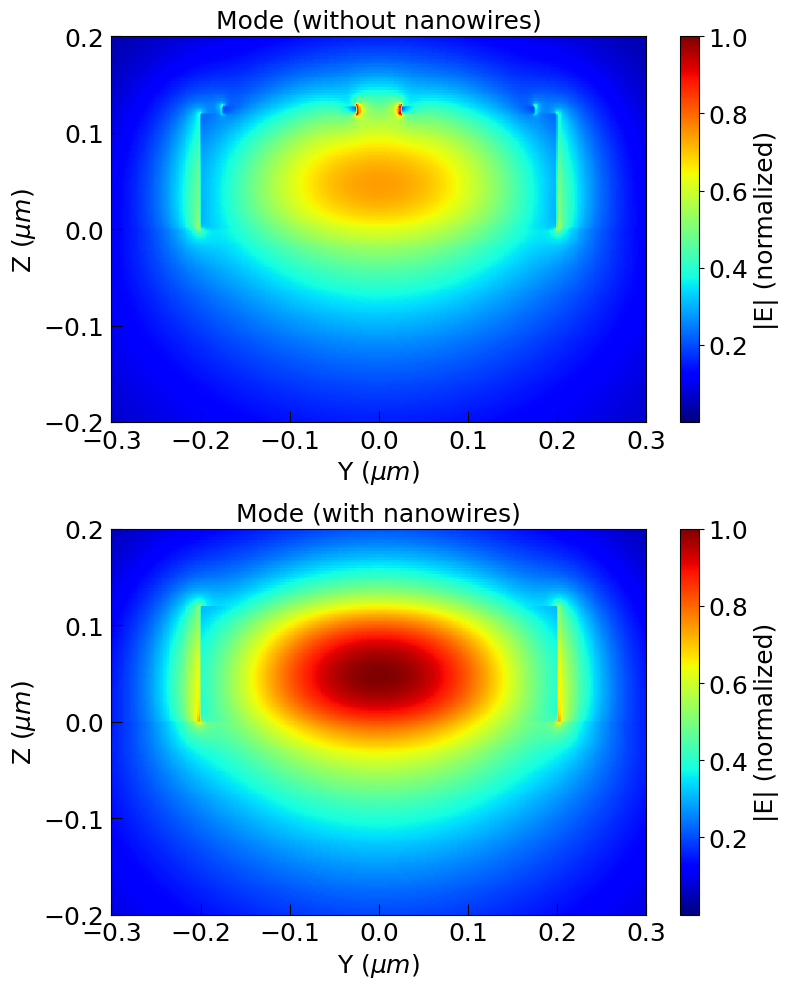
We have now designed and optimized the two hybrid nanophotonic components: the hBN nanowaveguide and the NbTiN SNSPD. With high coupling between a common silicon nitride photonic architecture and both a single-photon source and a single-photon detector, we can explore novel applications in quantum photonics. For further analysis of this data and the application of these structures in a full device, see Malinowski, K., Targholizadeh, A. et al. Overcoming the Classical Signal to Noise Ratio Limit Through On-Chip Photon Addition. APL Quantum 3, 026107 (2026) DOI: 10.1063/5.0314599.