The subminiature version A (SMA) coaxial connector is an essential component in printed circuit board (PCB) applications. It is commonly used as the interface between the on-board circuit and external components such as antennas or measurement devices.
In this notebook, we model two edge-mounted SMA connectors attached to a grounded co-planar waveguide (CPW). The connector-to-connector insertion and return losses are calculated to ensure proper impedance matching and minimal reflection.
import matplotlib.pyplot as plt
import numpy as np
import tidy3d as td
import tidy3d.rf as rf
from tidy3d import web

td.config.logging.level = "ERROR"
Building the Simulation
Key Parameters
# Frequencies and bandwidth
(f_min, f_max) = (1e9, 10e9)
f0 = (f_min + f_max) / 2
freqs = np.linspace(f_min, f_max, 301)
Important geometry dimensions are defined below. The default length unit is microns, so we introduce a mm conversion factor.
mm = 1000  # Conversion factor mm to microns

# Coaxial dimensions (50 ohm)
R0 = 0.635 * mm  # Coax inner radius
R1 = 2.125 * mm  # Coax outer radius

# Substrate overall dimensions
H = 1.57 * mm  # Substrate thickness
Lsub, Wsub = (83 * mm, 30 * mm)  # PCB board dimensions

# Transmission line dimensions
T = 0.038 * mm  #  Metal thickness
WS = 2.58 * mm  # Signal trace width
G = 1 * mm  # CPW gap width
WG = 5 * mm  # Side ground trace width

# Via dimensions
VR = 0.5 * mm  # Via radius
VP = 3 * mm  # Via pitch, longitudinal
VL = 3 * mm  # Via pitch, transverse
VS = 1 * mm  # Via start z-coordinate

# Edge mount dimensions
Voffset = 0.125 * mm  # SMA connector vertical offset
Medium and Structures
Below, we define the materials used in model:
- PTFE for the SMA dielectric core
- Gold for the SMA body
- FR4 for the PCB substrate
- Copper for the PCB traces
med_FR4 = td.Medium(permittivity=4.4)
med_PTFE = td.Medium(permittivity=2.1)
med_Cu = rf.LossyMetalMedium(conductivity=60, frequency_range=(f_min, f_max))  # [S/um]
med_Au = rf.LossyMetalMedium(conductivity=41, frequency_range=(f_min, f_max))  # [S/um]
The SMA geometry is imported from a STL file, and then translated and rotated to the appropriate position. The SMA core is created from a td.Cylinder instance. To ensure a close fit, we initialize the SMA core to be slightly larger than the inner radius and use Boolean subtraction to cut it to size.
# Import SMA geometry
geom_SMA = td.TriangleMesh.from_stl(filename="./misc/SMA_model.stl", scale=mm, origin=(0, 0, 0))
geom_SMA = (geom_SMA.rotated(np.pi / 2, 0)).rotated(np.pi, 2)
geom_SMA = geom_SMA.translated(0, Voffset, 0)

# Create SMA dielectric core
geom_SMA_diel = td.Cylinder(
    center=(0, Voffset, -6 * mm / 2), radius=1.1 * R1, length=6 * mm, axis=2
)
geom_SMA_diel -= geom_SMA
We also make a copy for a second connector.
# Make copy for second connector
geom_SMA2 = (geom_SMA.rotated(np.pi, 1)).translated(0, 0, Lsub)
geom_SMA_diel2 = (geom_SMA_diel.rotated(np.pi, 1)).translated(0, 0, Lsub)
The substrate and CPW geometries are created below.
# Substrate
geom_sub = td.Box.from_bounds(rmin=(-Wsub / 2, -H - T, 0), rmax=(Wsub / 2, -T, Lsub))

# Transmission line and connecting structures
geom_sig = td.Box.from_bounds(rmin=(-WS / 2, -T, 0), rmax=(WS / 2, 0, Lsub))
geom_gnd1 = td.Box.from_bounds(rmin=(-WS / 2 - G - WG, -T, 0), rmax=(-WS / 2 - G, 0, Lsub))
geom_gnd2 = geom_gnd1.reflected((1, 0, 0))
geom_line = td.GeometryGroup(geometries=[geom_sig, geom_gnd1, geom_gnd2])
geom_gnd = td.Box.from_bounds(rmin=(-Wsub / 2, -H - 2 * T, 0), rmax=(Wsub / 2, -H - T, Lsub))
To ensure proper transmission in the high frequency range, we create a via fence that encloses the signal trace.
# Create via fence
def create_via_hole(xpos, zpos):
    geom = td.Cylinder(center=(xpos, -H / 2 - T, zpos), axis=1, length=H, radius=VR)
    return geom


geom_via_array = []
zpos = VS
while zpos < Lsub - VS + 0.1 * mm:
    for xpos in [-VL, VL]:
        geom_via_array += [create_via_hole(xpos, zpos)]
    zpos += VP

geom_via_group = td.GeometryGroup(geometries=geom_via_array)
We combine the previously defined geometries and materials into Structure instances, ready for simulation.
# Create structures
str_SMA = td.Structure(geometry=geom_SMA, medium=med_Au)
str_SMA2 = td.Structure(geometry=geom_SMA2, medium=med_Au)
str_SMA_diel = td.Structure(geometry=geom_SMA_diel, medium=med_PTFE)
str_SMA_diel2 = td.Structure(geometry=geom_SMA_diel2, medium=med_PTFE)
str_sub = td.Structure(geometry=geom_sub, medium=med_FR4)
str_line = td.Structure(geometry=geom_line, medium=med_Cu)
str_gnd = td.Structure(geometry=geom_gnd, medium=med_Cu)
str_vias = td.Structure(geometry=geom_via_group, medium=med_Cu)

# List of all structures
structure_list = [
    str_SMA,
    str_SMA2,
    str_SMA_diel,
    str_SMA_diel2,
    str_sub,
    str_line,
    str_gnd,
    str_vias,
]
Grid and Boundaries
The simulation boundaries are open (PML) on all sides. We introduce a padding of wavelength/2 on all sides to ensure that the external boundaries do not encroach on the near-field.
# Define simulation size and center
padding = td.C_0 / f0 / 2
sim_LZ = Lsub + padding
sim_LX = Wsub + padding
sim_LY = 5 * mm + padding
sim_center = (0, 0, Lsub / 2)
The grid refinement strategy is as follows:
- Use
LayerRefinementSpecfor PCB metallic layers - Use
MeshOverrideStructurefor SMA dielectric core and metal via fences
# Define layer refinement spec
lr_options = {
    "corner_refinement": td.GridRefinement(dl=0.1 * mm, num_cells=2),
    "min_steps_along_axis": 1,
}
lr1 = rf.LayerRefinementSpec.from_structures(structures=[str_line], **lr_options)
lr2 = rf.LayerRefinementSpec.from_structures(structures=[str_gnd], **lr_options)

# Define mesh override around SMA core and vias
rbox1 = td.MeshOverrideStructure(
    geometry=geom_SMA_diel.bounding_box, dl=(0.2 * mm, 0.2 * mm, 0.2 * mm)
)
rbox2 = td.MeshOverrideStructure(
    geometry=geom_SMA_diel2.bounding_box, dl=(0.2 * mm, 0.2 * mm, 0.2 * mm)
)
rbox_vias = []
for geom in geom_via_array:
    rbox_vias += [
        td.MeshOverrideStructure(geometry=geom.bounding_box, dl=(0.3 * mm, None, 0.3 * mm))
    ]
The overall grid specification is defined below.
# Define overall grid specification
grid_spec = td.GridSpec.auto(
    min_steps_per_wvl=12,
    wavelength=td.C_0 / f_max,
    layer_refinement_specs=[lr1, lr2],
    override_structures=[rbox1, rbox2] + rbox_vias,
)
Monitors
We define some field monitors for visualization purposes below.
# Field Monitor
mon_1 = td.FieldMonitor(
    center=(0, -T - H / 2, 0),
    size=(td.inf, 0, td.inf),
    freqs=[f_min, f0, f_max],
    name="field in-plane",
)
mon_2 = td.FieldMonitor(
    center=(0, 0, 0),
    size=(0, td.inf, td.inf),
    freqs=[f_min, f0, f_max],
    name="field cross section",
)

# List of all monitors
monitor_list = [mon_1, mon_2]
Ports
Wave ports are positioned along the coaxial section of each SMA connector.
# Wave port position and dimension
wp_offset = 4 * mm  # longitudinal offset
w_port = 4.6 * mm  # port width and height

# Define wave ports
WP1 = rf.WavePort(
    center=(0, Voffset, -wp_offset),
    size=(w_port, w_port, 0),
    mode_spec=rf.MicrowaveModeSpec(target_neff=np.sqrt(2.1)),
    direction="+",
    name="WP1",
    frame=None,
)
WP2 = WP1.updated_copy(
    center=(0, Voffset, Lsub + wp_offset),
    direction="-",
    name="WP2",
)
Defining Simulation and TerminalComponentModeler
The Simulation and TerminalComponentModeler instances are defined below.
sim = td.Simulation(
    center=sim_center,
    size=(sim_LX, sim_LY, sim_LZ),
    grid_spec=grid_spec,
    structures=structure_list,
    monitors=monitor_list,
    run_time=5e-9,
    plot_length_units="mm",
    symmetry=(1, 0, 0),
)

tcm = rf.TerminalComponentModeler(
    simulation=sim,
    ports=[WP1, WP2],
    freqs=freqs,
)
Visualization
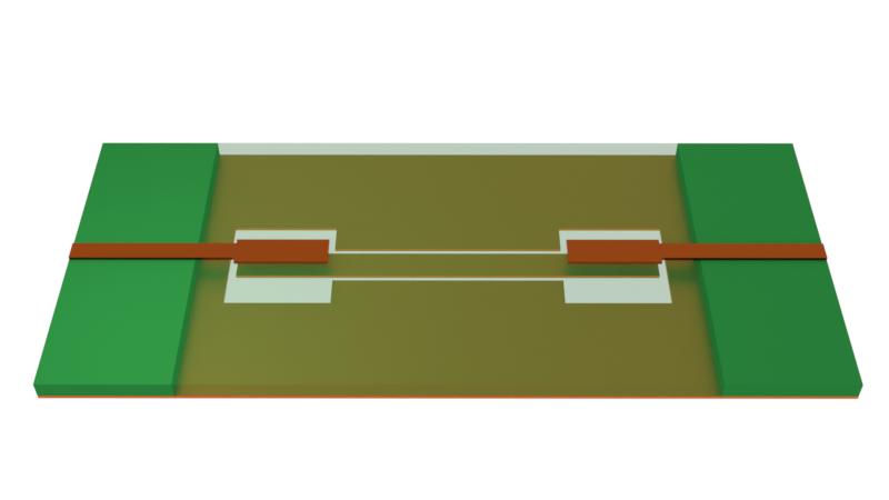
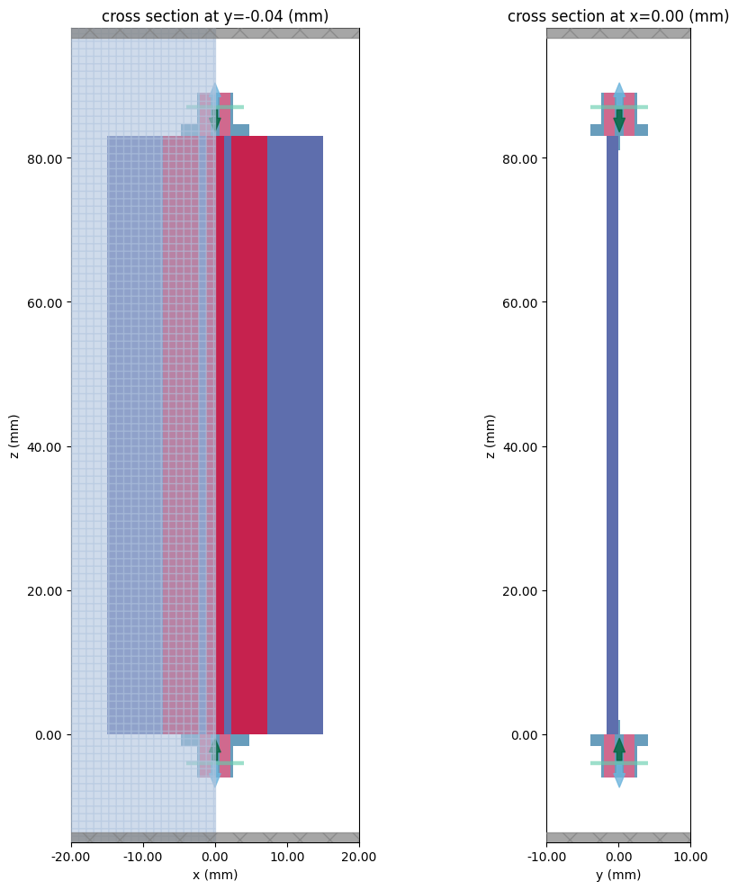
Before running, it is a good idea to check the structure layout and simulation grid. Below, the top and side cross-sections of the structure is shown, along with the wave ports sources (green arrow) and internal modal absorbers (blue arrow).
fig, ax = plt.subplots(1, 2, figsize=(10, 10), tight_layout=True)
tcm.plot_sim(
    y=-T, ax=ax[0], monitor_alpha=0, hlim=(-20 * mm, 20 * mm), vlim=(-15 * mm, Lsub + 15 * mm)
)
tcm.plot_sim(
    x=0, ax=ax[1], monitor_alpha=0, hlim=(-10 * mm, 10 * mm), vlim=(-15 * mm, Lsub + 15 * mm)
)
plt.show()
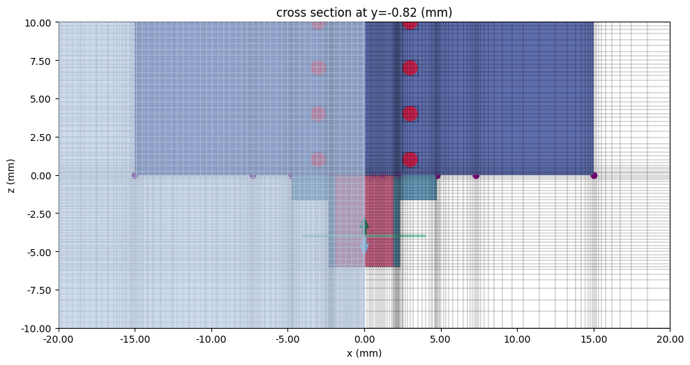
The grid in the SMA-CPW transition region is shown below. The mesh override regions are boxed with dotted black lines.
fig, ax = plt.subplots(figsize=(10, 10), tight_layout=True)
tcm.simulation.plot_grid(y=-T - H / 2, ax=ax)
tcm.plot_sim(
    y=-T - H / 2, ax=ax, monitor_alpha=0, hlim=(-20 * mm, 20 * mm), vlim=(-10 * mm, 10 * mm)
)
plt.show()
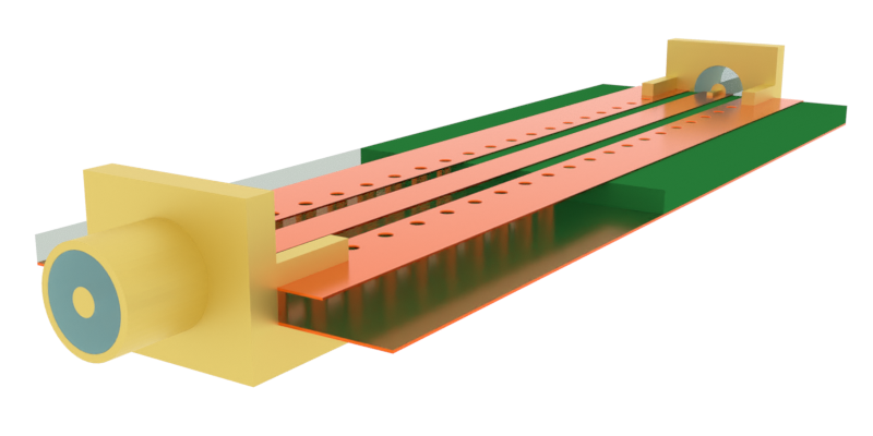
We can also visualize the setup in 3D.
sim.plot_3d()
Running the Simulation
The simulation is executed below.
tcm_data = web.run(tcm, task_name="sma_connector", path="data/sma_connector.hdf5")
15:22:00 EST Created task 'sma_connector' with resource_id
             'sid-3a8f78ea-f331-4fc3-9632-95aac852299d' and task_type
             'TERMINAL_CM'.
             View task using web UI at
             'https://tidy3d.simulation.cloud/rf?taskId=pa-42d6fa0a-82d8-4b0d-bc
             7e-89a78b3048ac'.
Task folder: 'default'.
Output()
15:22:08 EST Maximum FlexCredit cost: 0.350. Minimum cost depends on task
             execution details. Use 'web.real_cost(task_id)' after run.
15:22:09 EST Subtasks status - sma_connector
             Group ID: 'pa-42d6fa0a-82d8-4b0d-bc7e-89a78b3048ac'
Output()
Batch status = preprocess
15:22:15 EST Batch status = running
15:49:12 EST Batch status = postprocess
15:49:40 EST Modeler has finished running successfully.
Billed flex credit cost: 0.281.
Output()
15:49:46 EST Loading component modeler data from data/sma_connector.hdf5
Results
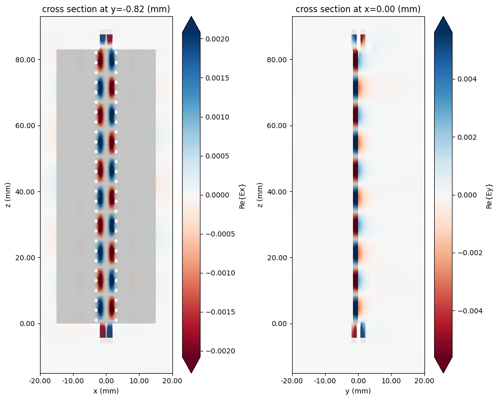
Field Profile
The field monitor data is accessed from the .data attribute of the TerminalComponentModelerData result. The key is in the format <wave port name>@<mode number>, for example WP1@0. (In this case, there is only one mode.)
# Extract simulation data
sim_data = tcm_data.data["WP1@0"]
Below, the Ex and Ey field components are plotted along the top and side cross-sections respectively.
fig, ax = plt.subplots(1, 2, figsize=(10, 8), tight_layout=True)
f_plot = f_max
sim_data.plot_field("field in-plane", field_name="Ex", val="real", f=f_plot, ax=ax[0])
sim_data.plot_field("field cross section", "Ey", val="real", f=f_plot, ax=ax[1])
for axis in ax:
    axis.set_ylim(-15 * mm, Lsub + 10 * mm)
    axis.set_xlim(-20 * mm, 20 * mm)
plt.show()
S-parameters
The S-matrix data is extracted using the smatrix() method. To access a specific S_ij parameter, use the corresponding port_in and port_out attributes. Note the use of np.conjugate to convert the S-parameter from the physics phase convention (current Tidy3D default) to the usual electrical engineering convention.
# Extract S-matrix and S-parameters
smat = tcm_data.smatrix()
S11 = np.conjugate(smat.data.isel(port_in=0, port_out=0))
S21 = np.conjugate(smat.data.isel(port_in=0, port_out=1))
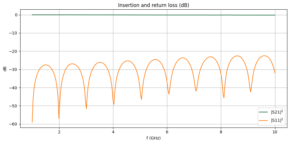
The insertion and return losses are plotted below. We observe excellent transmission and minimal reflection across the frequency band, indicating that the impedance of the SMA connector is well-matched to that of the on-board transmission line.
fig, ax = plt.subplots(figsize=(10, 5), tight_layout=True)
ax.plot(freqs / 1e9, 20 * np.log10(np.abs(S21)), label="|S21|$^2$")
ax.plot(freqs / 1e9, 20 * np.log10(np.abs(S11)), label="|S11|$^2$")
ax.set_title("Insertion and return loss (dB)")
ax.set_xlabel("f (GHz)")
ax.set_ylabel("dB")
ax.legend()
ax.grid()
plt.show()