Author: Yanyun Xue, Peking University
Electro-optic (EO) frequency combs, typically driven by microwave signals in $\chi^{(2)}$ materials, provide highly precise repetition rates in the microwave domain. However, their spectral span is fundamentally limited by the relatively weak EO interaction, implying that the role of dispersion is expected to be minor.
In this notebook, we show that even for state-of-the-art EO combs, the effect of dispersion remains negligible. As a representative example, Hu et al. reported a broadband EO comb with a 132-nm span in Nature Photonics (16, 679–685, 2022; https://doi.org/10.1038/s41566-022-01059-y ). Their device featured a line spacing of 30.925 GHz, corresponding to roughly 520 comb lines in total. In the following, we adopt the parameters from this work to analyze the impact of dispersion in EO combs.
This notebook is associated with the publication Lei, T., Song, Y., Xue, Y. et al. Strong-coupling and high-bandwidth cavity electro-optic modulation for advanced pulse-comb synthesis. Light Sci Appl 14, 373 (2025). DOI: 10.1038/s41377-025-02046-y.
import gdstk
import matplotlib.pyplot as plt
import numpy as np
import tidy3d as td
from tidy3d import web
from tidy3d.plugins.mode import ModeSolver
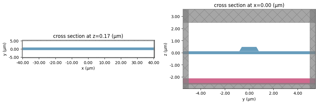
We choose the same stack and structure parameters as the original article.
# Define materials
n_SiO2 = 1.46
n_Si = 3.52
SiO2 = td.Medium(permittivity=n_SiO2**2)
Si = td.Medium(permittivity=n_Si**2)
LN_ye = td.material_library["LiNbO3"]["Zelmon1997"](1)
# Unit length is micron.
wg_height = 0.35
wg_width = 1.2
substrate_height = 0.25
SiO2_height = 2
Si_height = 0.5
wg_angle = 30 / 180 * np.pi

# Free-space wavelength (in um) and frequency (in Hz)
lambda0 = 1.603
freq0 = td.C_0 / lambda0
fwidth = freq0 / 10

# Simulation domain size and total run time
sim_length = 80
sim_size = [sim_length, 10, 5]

# Grid specification
grid_spec = td.GridSpec.auto(min_steps_per_wvl=40, wavelength=lambda0)
To define a waveguide with the correct sidewall angle, we will copy the auxiliary function defined in this example notebook.
def straight_waveguide(
    x0, y0, z0, x1, y1, wg_width, wg_thickness, medium, sidewall_angle=0
):
    """
    This function defines a straight strip waveguide and returns the tidy3d structure of it.

    Parameters
    ----------
    x0: x coordinate of the waveguide starting position (um)
    y0: y coordinate of the waveguide starting position (um)
    z0: z coordinate of the waveguide starting position (um)
    x1: x coordinate of the waveguide end position (um)
    y1: y coordinate of the waveguide end position (um)
    wg_width: width of the waveguide (um)
    wg_thickness: thickness of the waveguide (um)
    medium: medium of the waveguide
    sidewall_angle: side wall angle of the waveguide (rad)
    """

    cell = gdstk.Cell("waveguide")  # define a gds cell

    path = gdstk.RobustPath((x0, y0), wg_width, layer=1, datatype=0)  # define a path
    path.segment((x1, y1))

    cell.add(path)  # add path to the cell

    # define geometry from the gds cell
    wg_geo = td.PolySlab.from_gds(
        cell,
        gds_layer=1,
        axis=2,
        slab_bounds=(z0 - wg_thickness / 2, z0 + wg_thickness / 2),
        sidewall_angle=sidewall_angle,
    )

    # define tidy3d structure of the bend
    wg = td.Structure(geometry=wg_geo[0], medium=medium)

    return wg


# Structure
substrate = td.Structure(
    geometry=td.Box(
        center=[0, 0, 0],
        size=[td.inf, td.inf, substrate_height],
    ),
    medium=LN_ye,
)
substrate2 = td.Structure(
    geometry=td.Box(
        center=[0, 0, -substrate_height / 2 - SiO2_height / 2],
        size=[td.inf, td.inf, SiO2_height],
    ),
    medium=SiO2,
)
substrate3 = td.Structure(
    geometry=td.Box(
        center=[0, 0, -substrate_height / 2 - SiO2_height - Si_height / 2],
        size=[td.inf, td.inf, Si_height],
    ),
    medium=Si,
)
wg = straight_waveguide(
    x0=-50,
    y0=0,
    z0=(substrate_height + wg_height) / 2,
    x1=50,
    y1=0,
    wg_width=wg_width + wg_height * np.tan(wg_angle),
    wg_thickness=wg_height,
    medium=LN_ye,
    sidewall_angle=wg_angle,
)
# Modal source parameters
src_pos = 0
src_plane = td.Box(center=[src_pos, 0, substrate_height / 2 + 0.05], size=[0, 5, 2])
# define simulation
run_time = 40 / fwidth
sim = td.Simulation(
    center=(0, 0, 0),
    size=sim_size,
    grid_spec=grid_spec,
    structures=[substrate, substrate2, substrate3, wg],
    sources=[],
    monitors=[],
    run_time=run_time,
    boundary_spec=td.BoundarySpec.all_sides(boundary=td.Absorber()),
    medium=SiO2,
)

fig, (ax1, ax2) = plt.subplots(1, 2, tight_layout=True, figsize=(11, 4))
sim.plot(z=substrate_height / 2 + 0.05, ax=ax1)
sim.plot(x=0, ax=ax2)
plt.show()
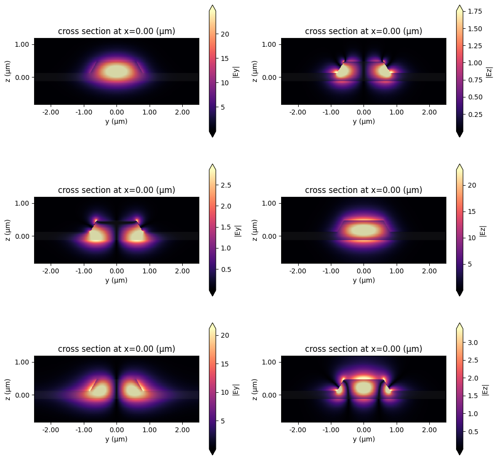
Next, we will run a ModeSolver analysis to verify the TE and TM modes.
# Visualize the modes
mode_spec = td.ModeSpec(
    num_modes=3,
    group_index_step=True,
)
ms = ModeSolver(simulation=sim, plane=src_plane, mode_spec=mode_spec, freqs=[freq0])
modes = web.run(ms, "mode_solver")
fig, axs = plt.subplots(3, 2, figsize=(12, 12))
for mode_ind in range(3):
    ms.plot_field("Ey", "abs", f=freq0, mode_index=mode_ind, ax=axs[mode_ind, 0])
    ms.plot_field("Ez", "abs", f=freq0, mode_index=mode_ind, ax=axs[mode_ind, 1])
modes.to_dataframe()

plt.show()
15:43:02 -03 Created task 'mode_solver' with task_id
             'mo-9628fa9d-816e-4b24-8dd2-9161b0f7ec71' and task_type
             'MODE_SOLVER'.
             View task using web UI at
             'https://tidy3d.simulation.cloud/workbench?taskId=mo-9628fa9d-816e-
             4b24-8dd2-9161b0f7ec71'.
Task folder: 'default'.
Output()
15:43:05 -03 Maximum FlexCredit cost: 0.007. Minimum cost depends on task
             execution details. Use 'web.real_cost(task_id)' to get the billed
             FlexCredit cost after a simulation run.
15:43:06 -03 status = success
Output()
15:43:17 -03 loading simulation from simulation_data.hdf5
modes.to_dataframe()
| wavelength | n eff | k eff | TE (Ey) fraction | wg TE fraction | wg TM fraction | mode area | group index | dispersion (ps/(nm km)) | ||
|---|---|---|---|---|---|---|---|---|---|---|
| f | mode_index | |||||||||
| 1.870196e+14 | 0 | 1.603 | 1.910956 | 0.0 | 0.995350 | 0.962768 | 0.898766 | 0.929827 | 2.261288 | -80.794706 |
| 1 | 1.603 | 1.897758 | 0.0 | 0.013627 | 0.816791 | 0.964912 | 1.153785 | 2.416122 | -241.893333 | |
| 2 | 1.603 | 1.781330 | 0.0 | 0.980359 | 0.900188 | 0.898879 | 1.502541 | 2.291297 | -698.173108 |
Finally, we can calculate use the dispersion parameter ($D_\lambda$) for calculating the second-order dispersion term and extrapolate to 260 comblines.
Group-velocity dispersion (GVD):
$$ \beta_2 = -D_\lambda \cdot \frac{\lambda_0 }{f_0 \cdot 2\pi} \quad [\text{ps}^2/\text{m}] $$
Second-order dispersion term for the resonator:
$$ D_2 = -\beta_2 \cdot \left(\frac{c_0 }{n_g}\right) \cdot ( \text{FSR} \cdot 2\pi )^2 $$
For the $n$-th sideband ($n=260$):
$$ \Delta f = \frac{D_2 \left[(n+1)^2 - n^2\right]}{2} $$
Relative frequency shift:
$$ \frac{\Delta f}{\text{FSR}} $$
Frequency variation across comb lines:
$$ \Delta f_R = \frac{D_2}{\text{FSR}} \cdot \frac{2m+1}{2} $$
# Show the free spectral range variation under the influence of dispersion
ng = modes.n_group_raw[0, 0]
FSR = 30.925e9  # 30.925GHz
dispersion = modes.dispersion_raw[0, 0] * 10 ** (-6)  # ps/m^2
beta2 = -dispersion * (lambda0 * 1e-6) / (freq0 * 2 * np.pi)  # ps^2/m
D2 = float(-beta2 * (td.C_0 * 1e-6 / ng) * (FSR * 2 * np.pi) ** 2)
n = 260  # the 260th sideband
delta_f = (D2 * (n + 1) ** 2 - D2 * (n) ** 2) / 2
relative_delta_f = delta_f / FSR
lines = np.linspace(-n, n, 2 * n + 1)
fR = (D2 / FSR) * (2 * lines + 1) / 2
plt.plot(lines, fR)
plt.xlabel("modes")
plt.ylabel("$\Delta f_R (f_R)$")
plt.title(rf"With {n} comblines span, $\Delta f_R$={abs(relative_delta_f):.7f}$f_R$")

plt.show()
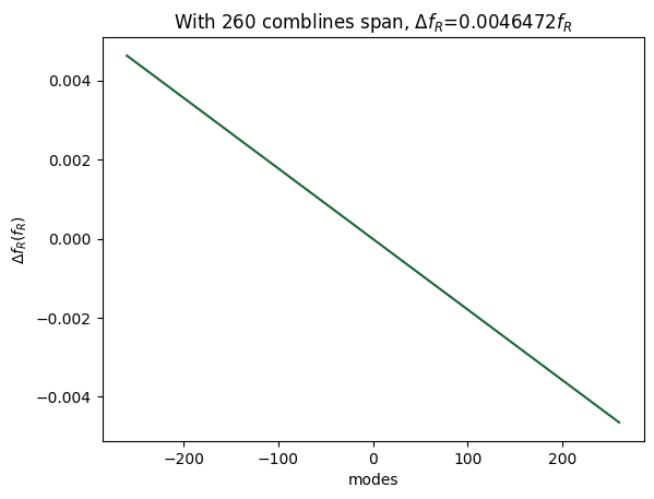
With 520 comblines span, $\Delta f_R=0.0050548 f_R=156$ MHz. If the intrinsic quality factor $Q_i=1M$, $\Delta f_R$ is less than the intrinsic linewidth $\kappa_i$. Therefore, the variation of repetition frequency can be neglected.