Author: Yazan Lampert, PhD student at Ecole Polytechnique Fédérale de Lausanne
Recent efforts have focused on matching the velocities of optical and microwave modes to demonstrate phase and intensity modulators with low loss and low $V_\pi$. Popular platforms include Lithium Niobate and organic silicon photonic platform. While such devices can operate at high speeds, frequencies above 500 GHz are not yet well studied. In this notebook, we simulate transmission lines that are phase-matched with the optical wavelength over the range [250 GHz - 5 THz]. This notebook is based on the paper: Photonics-integrated terahertz transmission lines. The transmission lines in this paper are used to provide efficient interaction between optical and terahertz pulses. The authors combined these structures with on-chip antennas to demonstrate terahertz generation and detection on-chip.

import matplotlib.pyplot as plt
import numpy as np
import tidy3d as td
import tidy3d.plugins.microwave as mw
import tidy3d.plugins.smatrix as sm
from tidy3d.plugins.dispersion import FastDispersionFitter
from tidy3d.plugins.mode import ModeSolver

td.config.logging_level = "ERROR"
Building the Simulation
Key Parameters
We begin by defining the frequency range for both the terahertz and the optical modes. We will run two separate simulations for each range.
## frequencies for the terahertz mode
# frequency range (Hz)
f_min, f_max = (250e9, 5e12)

# center frequency
f0 = (f_max + f_min) / 2

# frequency sampling points
freqs = np.linspace(f_min, f_max, 50)

## frequencies for the optical mode
# wavelength range [um]
wl_min, wl_max = (1.480, 1.620)

nu_min, nu_max = (td.C_0 / wl_max, td.C_0 / wl_min)

# center optical frequency
nu0 = (nu_min + nu_max) / 2

# optical frequency sampling points
opt_freqs = np.linspace(nu_min, nu_max, 50)
Next, we define the entire structure which is shown in detail in the supplementary material of the referenced paper. The structure consists of a photonic waveguide that is placed between two gold striplines. The optical waveguide is for guiding the optical mode and the striplines are a transmission line for the terahertz mode.
# geometry
w_TL = 3.5  # signal strip width
h_TL = 0.3  # transmission line thickness
L = 5  # length of structure

h_cladding = 1  # cladding thickness
h_opening = h_cladding - h_TL  # opening above the stripline

w_g = 3.3  # gap between edge-coupled pair

h_SiO2 = 4.7  # oxide thickness
h_Si = 2  # substrate thickness

h_TF = 0.3  # thin-film lithium niobate thickness

h_wg = 0.3  # waveguide height
wg_w = 1.85  # waveguide width

entire_height = h_Si + h_SiO2 + h_TF + h_wg + h_opening  # entire structure height

len_inf = 1e6  # effective infinity
Due to strong dispersion, material properties must be defined separately for optical and terahertz frequencies.
# terahertz material properties
cond = 49  # Conductivity of gold in S/um

## for Lithium Niobate
eps_inf = 0.95
w = 2 * np.pi * freqs / 1e12 / 1000  # (rad/fs or rad THz /1000)
A = 2.027e1  # (rad/fs)
B = 1.068e1  # (rad/fs)
eps1 = 16.6
eps2 = 2.6
omega_0_1 = 4.7e-2  # (rad/fs)
omega_0_2 = 1.19e-1  # (rad/fs)
delta_0_1 = 2.3e-3  # (rad/fs)
delta_0_2 = 2.8e-3  # (rad/fs)
epsilon_complex = (
    eps_inf
    + A**2 / (B**2 - w**2)
    + eps1 * omega_0_1**2 / (omega_0_1**2 - 2j * delta_0_1 * w - w**2)
    + eps2 * omega_0_2**2 / (omega_0_2**2 - 2j * delta_0_2 * w - w**2)
)
epsilon_r = np.real(epsilon_complex)
epsilon_i = np.imag(epsilon_complex)

n_Si_THz = 3.41
n_SiO2_THz = 1.9599

Si_THz = td.Medium(permittivity=n_Si_THz**2)
SiO2_THz = td.Medium(permittivity=n_SiO2_THz**2)


LN_e_THz = FastDispersionFitter.constant_loss_tangent_model(
    epsilon_r,
    epsilon_i / epsilon_r,
    (f_min, f_max),
    number_sampling_frequency=len(freqs),
    tolerance_rms=2e-4,
)


LN = td.material_library["LiNbO3"]["Zelmon1997"]
LN_e_opt = LN(1)

sio2_opt = td.material_library["SiO2"]["Horiba"]
si_opt = td.material_library["cSi"]["Li1993_293K"]

air = td.Medium(permittivity=1.0)
Output()
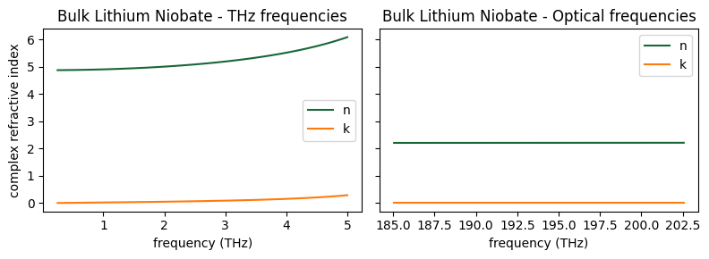
When plotting the refractive indices for both ranges, we notice that there is a great mismatch between optical and terahertz frequencies. This variation is due to the strong dispersion of lithium niobate compared to material such as silicon and silicon oxide.
fig, ax_plot = plt.subplots(1, 2, figsize=(8, 3), sharey=True, tight_layout=True)
LN_e_THz.plot(freqs, ax=ax_plot[0])
LN_e_opt.zz.plot(opt_freqs, ax=ax_plot[1])
ax_plot[0].set_ylabel("complex refractive index")
ax_plot[0].set_title("Bulk Lithium Niobate - THz frequencies")
ax_plot[1].set_title("Bulk Lithium Niobate - Optical frequencies")

plt.show()
Terahertz Simulation
Now that we have defined the materials, we will create the structures. For the optical simulation, we will keep the structures and update the refractive indices. This is done after the terahertz simulation.
# metal medium which is needed for the terahertz mode
med_metal = td.LossyMetalMedium(
    conductivity=cond, frequency_range=(f_min, f_max), name="Metal"
)
med_metal = med_metal.updated_copy(viz_spec=td.VisualizationSpec(facecolor="#edbe26"))

# silicon dioxide below thin-film lithium niobate layer
oxide_box = td.Structure(
    geometry=td.Box(
        center=(0, -h_TL / 2 - h_TF - h_SiO2 / 2, 0), size=(len_inf, h_SiO2, len_inf)
    ),
    medium=SiO2_THz,
    name="oxide",
)

# thin-film lithium niobate layer
TFLN = td.Structure(
    geometry=td.Box(center=(0, -h_TL / 2 - h_TF / 2, 0), size=(len_inf, h_TF, len_inf)),
    medium=LN_e_THz,
    name="TFLN",
)

# due to fabrication constraints, the waveguide has sidewalls at an angle of 30 degrees
sidewall_angle = 30
points = np.array(
    [
        (-wg_w / 2, -h_wg / 2),
        (wg_w / 2, -h_wg / 2),
        (wg_w / 2 - np.tan(np.pi * sidewall_angle / 180) * h_wg, h_wg / 2),
        (-wg_w / 2 + np.tan(np.pi * sidewall_angle / 180) * h_wg, h_wg / 2),
    ]
)
wg = td.Structure(
    geometry=td.PolySlab(vertices=points, axis=2, slab_bounds=(-L / 2, L / 2)),
    medium=LN_e_THz,
    name="waveguide",
)

# substrate
str_sub = td.Structure(
    geometry=td.Box(
        center=(0, -h_TL / 2 - h_TF - h_SiO2 - h_Si / 2, 0),
        size=(len_inf, h_Si, len_inf),
    ),
    medium=Si_THz,
    name="substrate",
)

# left transmission line strip
str_strip_left = td.Structure(
    geometry=td.Box(center=(-(w_g + w_TL) / 2, 0, 0), size=(w_TL, h_TL, len_inf)),
    medium=med_metal,
    name="left TL",
)

# Right transmission line strip
str_strip_right = td.Structure(
    geometry=td.Box(center=((w_g + w_TL) / 2, 0, 0), size=(w_TL, h_TL, len_inf)),
    medium=med_metal,
    name="right TL",
)

# opening above left transmission line strip
left_opening = td.Structure(
    geometry=td.Box(
        center=(-(w_g + w_TL) / 2, h_TL / 2 + h_opening / 2, 0),
        size=(w_TL, h_opening, len_inf),
    ),
    medium=air,
    name="left_opening_TL",
)

# opening above right transmission line strip
right_opening = td.Structure(
    geometry=td.Box(
        center=((w_g + w_TL) / 2, h_TL / 2 + h_opening / 2, 0),
        size=(w_TL, h_opening, len_inf),
    ),
    medium=air,
    name="right_opening_TL",
)
Grid and Boundaries
The LayerRefinementSpec feature is useful for refining the grid around metallic structures as it automatically detects metal edges and corners.
# create a LayerRefinementSpec from structures
lr_spec = td.LayerRefinementSpec.from_structures(
    structures=[str_strip_left, str_strip_right],
    axis=1,  # layer normal is in y-direction
    min_steps_along_axis=10,  # min  grid cells along normal direction
    refinement_inside_sim_only=False,  # metal structures extend outside sim domain. Set 'False' to snap to corners outside sim.
    bounds_snapping="bounds",  # snap grid to metal boundaries
    corner_refinement=td.GridRefinement(dl=h_TL / 20, num_cells=2),
)

# the rest of the grid is automatically generated based on the wavelength.
grid_spec = td.GridSpec.auto(
    wavelength=td.C_0 / f_max,
    min_steps_per_wvl=50,
    layer_refinement_specs=[lr_spec],
)

# perfectly matched layers for the boundaries
boundary_spec = td.BoundarySpec(
    x=td.Boundary.pml(),
    y=td.Boundary.pml(),
    z=td.Boundary.pml(),
)
Wave Ports
# define port specification
wave_port_mode_spec = td.ModeSpec(num_modes=2, target_neff=2.2)

# define current and voltage integrals
current_integral = mw.CurrentIntegralAxisAligned(
    center=((w_g + w_TL) / 2, 0, -L / 2), size=(w_TL + w_g, 4 * h_TL, 0), sign="+"
)
voltage_integral = mw.VoltageIntegralAxisAligned(
    center=(0, 0, -L / 2),
    size=(w_g, 0, 0),
    extrapolate_to_endpoints=True,
    snap_path_to_grid=True,
    sign="+",
)

# Define wave ports
WP1 = sm.WavePort(
    center=(0, 0, -L / 2),
    size=(len_inf, len_inf, 0),
    mode_spec=wave_port_mode_spec,
    direction="+",
    name="WP1",
    mode_index=0,
    current_integral=current_integral,
    voltage_integral=voltage_integral,
)
WP2 = WP1.updated_copy(
    name="WP2",
    center=(0, 0, L / 2),
    direction="-",
    current_integral=current_integral.updated_copy(
        center=((w_g + w_TL) / 2, 0, L / 2), sign="-"
    ),
    voltage_integral=voltage_integral.updated_copy(center=(0, 0, L / 2)),
)
Define the Terahertz Simulation
The Simulation object in Tidy3D contains information about the entire simulation environment, including boundary conditions, grid, structures, and monitors.
sim_thz = td.Simulation(
    size=(4 * w_TL, entire_height, 1.01 * L),
    center=(0, (h_cladding + h_opening - entire_height) / 2, 0),
    grid_spec=grid_spec,
    boundary_spec=boundary_spec,
    structures=[
        str_sub,
        str_strip_left,
        str_strip_right,
        wg,
        TFLN,
        oxide_box,
        left_opening,
        right_opening,
    ],
    monitors=[],
    run_time=5e-12,  # simulation run time in seconds
    shutoff=1e-7,  # lower shutoff threshold for more accuracy at low frequencies
    plot_length_units="um",
    medium=SiO2_THz,  # background_medium is silicon dioxide
)
Before running the simulation, it is recommended to verify that the structures have been created properly.
# inspect transverse grid
fig, ax = plt.subplots(figsize=(10, 6))
sim_thz.plot(z=1, ax=ax)

# 3D plot of the simulation structure
sim_thz.plot_3d()

plt.show()

2D Analysis
To obtain all the key transmission line parameters, such as attenuation $\alpha$, characteristic impedance $Z_0$, and effective index $n_{\text{eff}}$, we perform a 2D ModeSolver calculation.
# convert wave port to mode solver
mode_solver_thz = WP1.to_mode_solver(sim_thz, freqs)
We execute the mode solver study below.
mode_data_thz = td.web.run(mode_solver_thz, task_name="mode solver for terahertz mode")
15:41:11 -03 Created task 'mode solver for terahertz mode' with resource_id
             'mo-11a589e2-144d-40bc-b495-cc768e069709' and task_type
             'MODE_SOLVER'.
             View task using web UI at
             'https://tidy3d.simulation.cloud/workbench?taskId=mo-11a589e2-144d-
             40bc-b495-cc768e069709'.
Task folder: 'default'.
Output()
15:41:16 -03 Estimated FlexCredit cost: 0.011. Minimum cost depends on task
             execution details. Use 'web.real_cost(task_id)' to get the billed
             FlexCredit cost after a simulation run.
15:41:18 -03 status = queued
             To cancel the simulation, use 'web.abort(task_id)' or
             'web.delete(task_id)' or abort/delete the task in the web UI.
             Terminating the Python script will not stop the job running on the
             cloud.
Output()
15:41:23 -03 starting up solver
15:41:24 -03 running solver
15:41:52 -03 status = success
             View simulation result at
             'https://tidy3d.simulation.cloud/workbench?taskId=mo-11a589e2-144d-
             40bc-b495-cc768e069709'.
Output()
15:42:01 -03 loading simulation from simulation_data.hdf5
A great advantage of this transmission line structure is that it provides the same mode shape over the entire frequency range from 250 GHz up to 5 THz.
fig, ax = plt.subplots(5, 1, figsize=(11, 11), tight_layout=True)
frequencies_to_plot = [250e9, 500e9, 1e12, 3e12, 5e12]
for k, axis in enumerate(ax):
    mode_solver_thz.plot_field(
        field_name="Ex", val="real", mode_index=0, f=frequencies_to_plot[k], ax=axis
    )
    axis.set_title(f"Re(Ex) at {frequencies_to_plot[k] / 1e12} THz")
    axis.set_ylim(-6, 1)

plt.show()

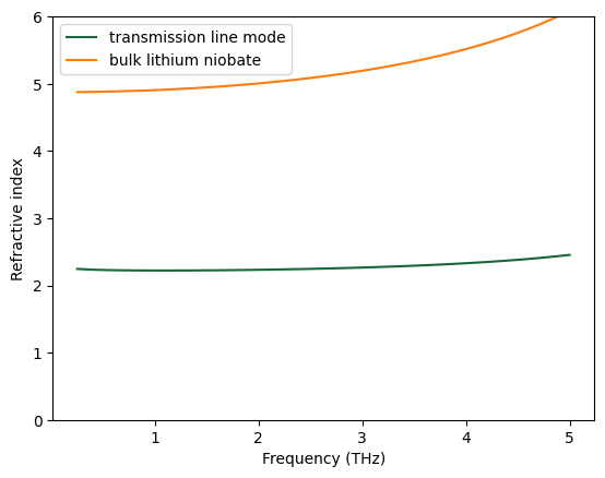
Next, we plot the effective index for the first mode and compare it to the refractive index of bulk lithium niobate.
fig, ax = plt.subplots()
neff_mode = mode_data_thz.modes_info["n eff"].squeeze()
ax.plot(freqs * 1e-12, neff_mode[:, 0], label="transmission line mode")

# get the complex permittivity from the fitted model
eps_complex = LN_e_THz.eps_model(freqs)

# convert to refractive index (n + ik)
n_complex = np.sqrt(eps_complex)

# extract only the real part
n_real = np.real(n_complex)

ax.plot(freqs * 1e-12, n_real, label="bulk lithium niobate")
plt.legend()
plt.ylim(0, 6)
plt.ylabel("Refractive index")
plt.xlabel("Frequency (THz)")

plt.show()
The mode solver solution data includes $n_{\text{eff}}$ and attenuation $\alpha$ in dB/cm. From this, we can also derive the real part of the propagation constant, $\beta$, as well as the complex propagation constant $\gamma$.
neff_mode = mode_data_thz.modes_info["n eff"].squeeze()
alphadB_mode = mode_data_thz.modes_info["loss (dB/cm)"].squeeze()
# calculate beta, alpha (in 1/um), and gamma
beta_mode = 2 * np.pi * freqs * neff_mode[:, 0] / td.C_0
alpha_mode = alphadB_mode / 8.686 / 1e4
gamma_mode = alpha_mode + 1j * beta_mode
We obtain $Z_0$ by calling the compute_impedance() method in the ImpedanceCalculator class, making use of the previously defined current and voltage integrals.
Z0_mode = (
    mw.ImpedanceCalculator(
        voltage_integral=voltage_integral, current_integral=current_integral
    )
    .compute_impedance(mode_data_thz)
    .isel(mode_index=0)
)
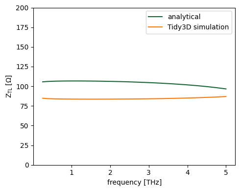
We can show that the simulation results give similar values to an analytical model from Garg, Ramesh, and Inder J. Bahl. Microstrip lines and slotlines. Artech House, 2024.
\begin{equation} Z_{TL}=\frac{120 \pi}{ \sqrt{\varepsilon_{eff}}} \frac{k}{k'} \end{equation}
where $k' = \sqrt{\,1 - k^2\,} $ and the parameter $k$ is determined by the dimensions of the transmission line: $k =\frac{w_g}{w_{TL}+2\cdot w_g} $
s = w_g * 1e-6
w = w_TL * 1e-6
k = s / (s + 2 * w)
k_prime = np.sqrt(1 - k**2)

K_ratio = np.pi / np.log(2 * (1 + np.sqrt(k_prime)) / (1 - np.sqrt(k_prime)))
Z_0_analytical = 120 * np.pi / neff_mode[:, 0] * K_ratio

fig, ax = plt.subplots(figsize=(5, 4), tight_layout=True)

Z_simulation = Z0_mode.real
plt.plot(freqs * 1e-12, Z_0_analytical, label="analytical")
plt.plot(freqs * 1e-12, Z_simulation, label="Tidy3D simulation")

plt.ylim(0, 200)
plt.xlabel("frequency [THz]")
plt.ylabel(r"$\mathrm{Z_{TL}}$ [Ω]")
plt.legend()

plt.savefig("Z_TL.pdf", format="pdf", transparent=True)

plt.show()
Optical Simulation
To determine phase matching between optical and terahertz modes, we run an optical simulation to determine the group index at telecom frequencies.
# silicon dioxide below thin-film lithium niobate layer
oxide_box = oxide_box.updated_copy(medium=sio2_opt)

# thin-film lithium niobate layer
TFLN = TFLN.updated_copy(medium=LN_e_opt)

# waveguide
wg = wg.updated_copy(medium=LN_e_opt)

# substrate
str_sub = str_sub.updated_copy(medium=si_opt)
We will consider the gold stripline to be a perfect electrical conductor for the optical frequencies.
# left transmission line strip
str_strip_left = str_strip_left.updated_copy(medium=td.PEC)

# right transmission line strip
str_strip_right = str_strip_right.updated_copy(medium=td.PEC)
The grid specification for the optical simulation is automatic.
# define overall grid specification
grid_spec = td.GridSpec.auto(wavelength=td.C_0 / nu_max, min_steps_per_wvl=50)
Since we know that the optical mode will be confined inside the waveguide, we define the simulation domain to be around the lithium niobate waveguide.
sim_opt = td.Simulation(
    size=(3 * wg_w, h_wg * 5, 1.01 * L),
    center=(0, 0, 0),
    grid_spec=grid_spec,
    boundary_spec=boundary_spec,
    structures=[
        str_sub,
        str_strip_left,
        str_strip_right,
        wg,
        TFLN,
        oxide_box,
        left_opening,
        right_opening,
    ],
    monitors=[],
    run_time=5e-12,  # simulation run time in seconds
    shutoff=1e-7,  # lower shutoff threshold for more accuracy at low frequency
    plot_length_units="um",
    medium=sio2_opt,  # background_medium is silicon dioxide
)
The goal of such structures is to exploit the nonlinear $d_{333}$ coefficient of lithium niobate. This tensor coefficient is along the z-axis of the crystal (x-axis in the simulation). Therefore, we are only interested in the TE polarization of the optical mode.
mode_spec = td.ModeSpec(
    filter_pol="te",
    precision="double",
    num_pml=(5, 5),
    group_index_step=True,
    num_modes=2,
)

plane = td.Box(
    center=(0, 0, -L / 2), size=(1.8 * wg_w, h_wg * 4, 0)
)  # create simulation plane

mode_solver_opt = ModeSolver(
    simulation=sim_opt,
    plane=plane,
    mode_spec=mode_spec,
    freqs=opt_freqs,
)
fig, ax = plt.subplots(figsize=(10, 6))
sim_opt.plot(z=1, ax=ax)
plt.show()
# 3D plot of the simulation structure
sim_opt.plot_3d()

plt.show()

mode_data_opt = td.web.run(mode_solver_opt, task_name="mode solver for optical mode")
15:42:04 -03 Created task 'mode solver for optical mode' with resource_id
             'mo-88baaa1b-f70c-4f29-84c1-1d51d076884a' and task_type
             'MODE_SOLVER'.
             View task using web UI at
             'https://tidy3d.simulation.cloud/workbench?taskId=mo-88baaa1b-f70c-
             4f29-84c1-1d51d076884a'.
Task folder: 'default'.
Output()
15:42:07 -03 Estimated FlexCredit cost: 0.014. Minimum cost depends on task
             execution details. Use 'web.real_cost(task_id)' to get the billed
             FlexCredit cost after a simulation run.
15:42:09 -03 status = queued
             To cancel the simulation, use 'web.abort(task_id)' or
             'web.delete(task_id)' or abort/delete the task in the web UI.
             Terminating the Python script will not stop the job running on the
             cloud.
Output()
15:42:14 -03 starting up solver
running solver
15:43:11 -03 status = success
             View simulation result at
             'https://tidy3d.simulation.cloud/workbench?taskId=mo-88baaa1b-f70c-
             4f29-84c1-1d51d076884a'.
Output()
15:43:23 -03 loading simulation from simulation_data.hdf5
Final Results
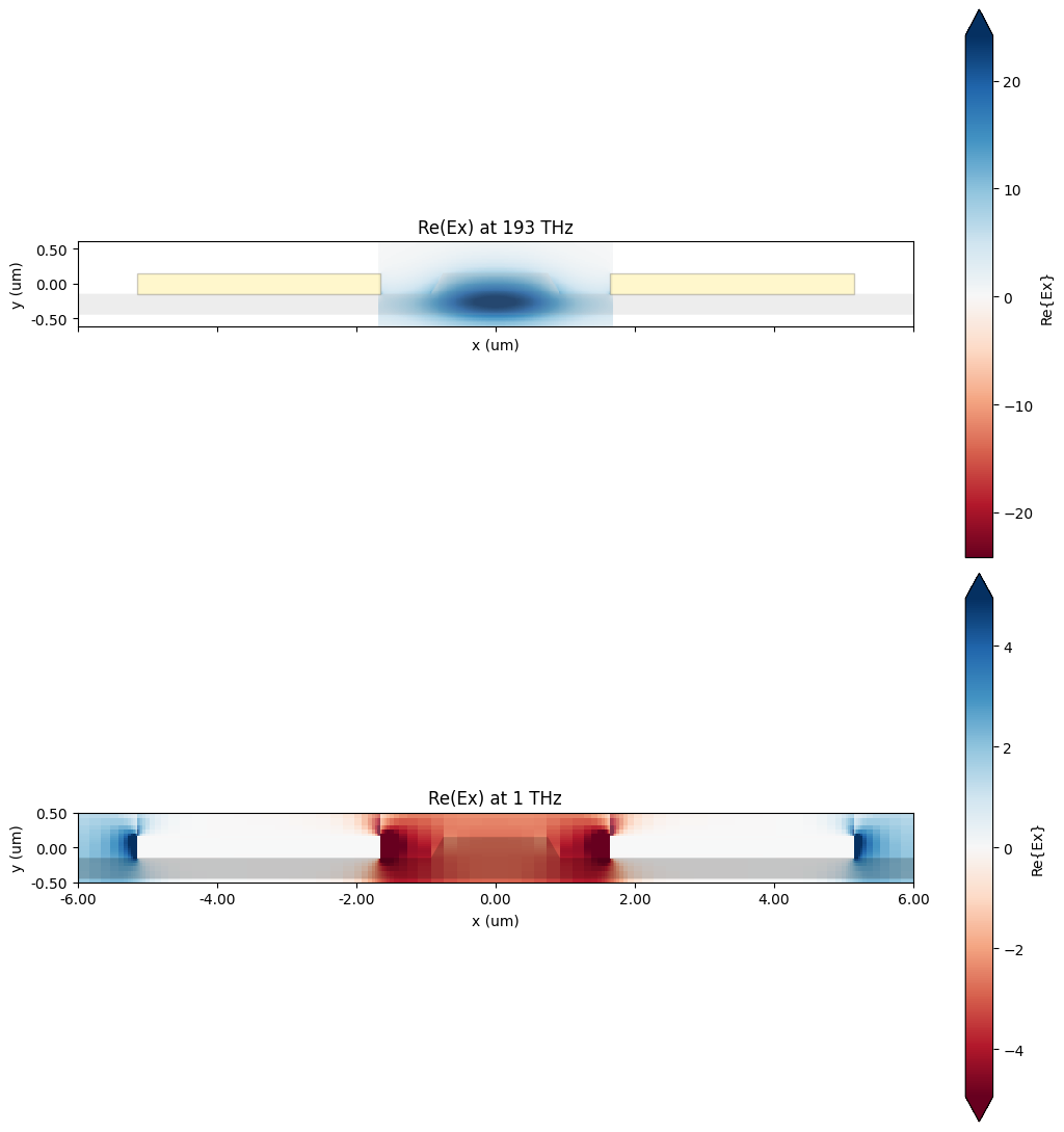
We can plot both the optical and terahertz mode to show how they overlap mainly inside the gap of transmission line.
fig, ax = plt.subplots(2, 1, figsize=(11, 11), sharex=True, tight_layout=True)

mode_solver_opt.plot_field(
    field_name="Ex", val="real", mode_index=0, f=193e12, ax=ax[0]
)
ax[0].set_title("Re(Ex) at 193 THz")
mode_solver_thz.plot_field(field_name="Ex", val="real", mode_index=0, f=1e12, ax=ax[1])
ax[1].set_title("Re(Ex) at 1 THz")
ax[0].set_xlim(-6, 6)
ax[1].set_ylim(-0.5, 0.5)

plt.show()
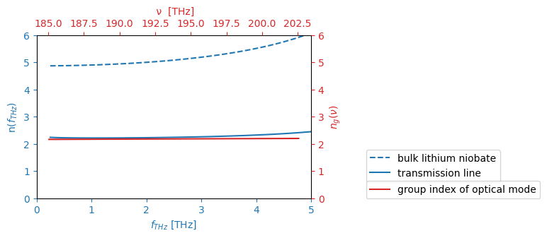
Now, we can extract all refractive indices. We already plotted the terahertz refractive index. Let us extract the optical group index. By doing so, we can reproduce Fig. 1 c in the main article.
group_index = mode_data_opt.n_group[:, 0]


fig = plt.figure(figsize=(5, 3))
ax1 = fig.add_subplot(111, label="1")
ax2 = fig.add_subplot(111, label="2", frame_on=False)

color = "tab:blue"
ax1.set_xlabel("$f_{THz}$ [THz]", color=color)
ax1.set_ylabel("n($f_{THz}$)", color=color)  # we already handled the x-label with ax1
ax1.plot(freqs * 1e-12, n_real, "--", color=color, label="bulk lithium niobate")
ax1.plot(freqs * 1e-12, neff_mode[:, 0], "-", color=color, label="transmission line")


ax1.tick_params(axis="y", labelcolor=color)
ax1.tick_params(axis="x", colors=color)
ax1.tick_params(axis="y", colors=color)
ax1.set_ylim(0, 6)
ax1.set_xlim(0, 5)
ax1.legend(loc=(1.2, 0.1))

color = "tab:red"
ax2.set_xlabel(" ν  [THz]", color=color)
ax2.yaxis.tick_right()
ax2.set_ylabel("$n_g(ν)$", color=color)
ax2.xaxis.tick_top()
ax2.xaxis.set_label_position("top")
ax2.yaxis.set_label_position("right")
ax2.plot(
    opt_freqs * 1e-12,
    group_index,
    "-",
    color=color,
    label="group index of optical mode",
)
ax2.tick_params(axis="y", labelcolor=color)
ax2.tick_params(axis="x", colors=color)
ax2.tick_params(axis="y", colors=color)
ax2.set_ylim(0, 6)


ax2.legend(loc=(1.2, 0))
plt.grid(False)
plt.savefig("ref_index.pdf", format="pdf", transparent=True)

plt.show()
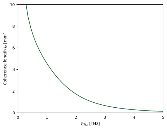
Finally, we determine the coherence length which is given by the formula $l_c=\frac{c_0}{2 f |n_g - n_{TL}|}$. This parameter determines the length at which the phase mismatch reaches 180° between the terahertz and optical waves. For the optical mode, we will choose the group index at 193 THz.
c_0 = 299792458
n_g = group_index[25].item()
l_c = c_0 / (2 * freqs * np.abs(neff_mode[:, 0] - n_g))  # in m
plt.plot(freqs * 1e-12, l_c * 1e3)
plt.ylim(0, 10)
plt.xlim(0, 5)
plt.xlabel("$f_{THz}$ [THz]")
plt.ylabel("Coherence length $l_c$ [mm]")

plt.show()