Note: this notebook requires Tidy3D version 2.10.0 or later.
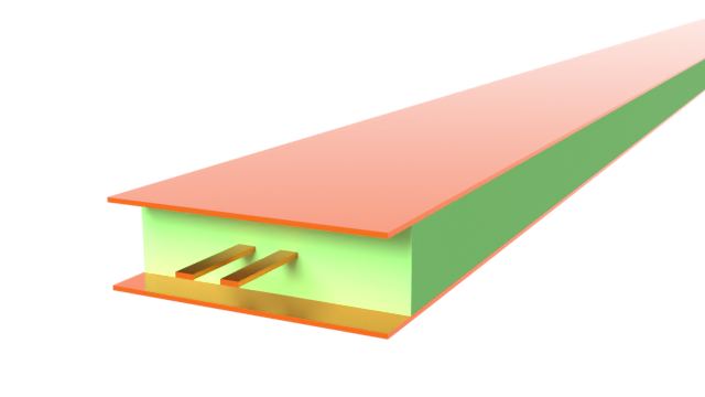
The co-planar waveguide (CPW) is a transmission line commonly used in RF photonics due to its compact planar nature, ease of fabrication, and resistance to external EM interference. In this notebook series, we will examine the CPW in the context of a Mach-Zehnder modulator (MZM).
In part one, we started with a simple CPW on a dielectric substrate. The goal of the notebook is to demonstrate the typical 2D and 3D workflow in Tidy3D's RF solver. We also benchmarked key results against other commercial RF simulation software.
In part two (this notebook), we will simulate the CPW with the MZM optical waveguide. A 2D mode analysis will first be performed on the conventional straight CPW layout, followed by a 3D simulation of a segmented electrode design. The latter will be benchmarked against a commercial FEM code. In the final section, we compare the Flexcompute RF solver next to experimental results from R&D developments of a Lithium Tantalate–based PDK at Luxtelligence SA.
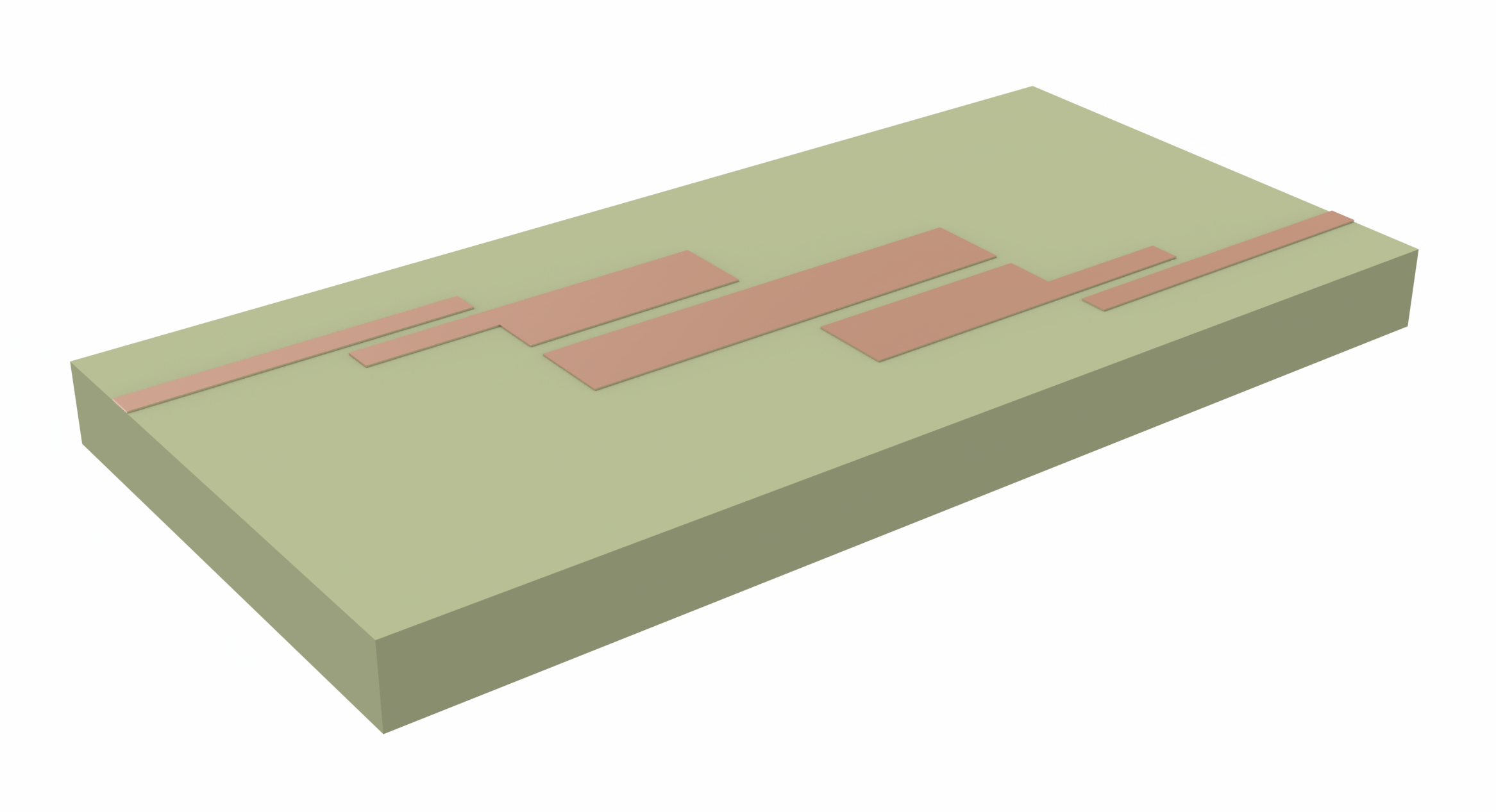
The segmented electrode design aims to address two key shortcomings of the conventional CPW: velocity mismatch and metallic loss. It is formed by adding T-shaped metal electrodes to the gaps in a conventional CPW. The effective RF index can be tuned by changing the T-electrode geometry, thus allowing for ideal velocity matching between the electrical and optical signals. The T-electrodes also spread the RF surface current outwards away from the gap, effectively increasing conductor area and reducing overall loss. At the same time, the CPW gap remains narrow in order to maintain a strong RF field for optical modulation.
import matplotlib.pyplot as plt
import numpy as np
import tidy3d as td
import tidy3d.rf as rf
from tidy3d import web

td.config.logging.level = "ERROR"
Key Parameters and Mediums
We define some general model parameters below. The analysis bandwidth is between 1 and 65 GHz.
# Frequency range
f_min, f_max = (1e9, 65e9)
f0 = (f_min + f_max) / 2
freqs = np.linspace(f_min, f_max, 101)
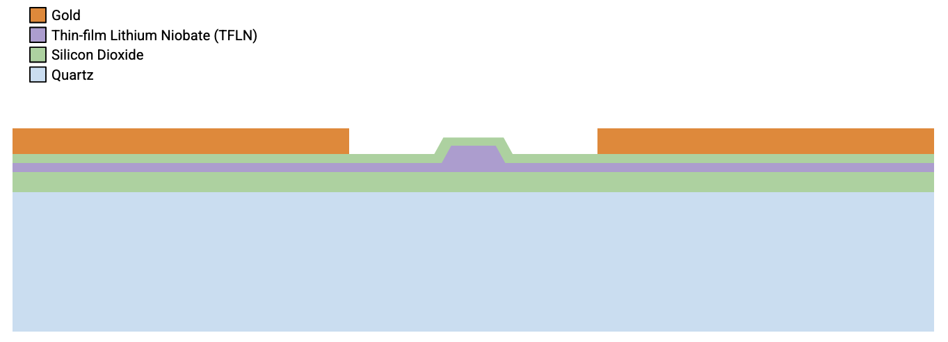
The material properties are defined below. The optical waveguide is made of thin-film lithium niobate (TFLN) with SiO2 cladding. The substrate is made of quartz. The metal CPW electrodes are made of gold.
The anisotropic TFLN is implemented with the AnisotropicMedium feature.
We assume gold to be the only lossy medium in this study, as conductor losses typically dominate in the the bandwidth of interest. In order to implement constant loss over the frequency range, we use LossyMetalMedium which implements a surface impedance model (SIBC) with constant conductivity.
# Mediums
med_air = td.Medium(permittivity=1, name="Air")
med_SiO2 = td.Medium(permittivity=3.8, name="SiO2")
med_Qz = td.Medium(permittivity=4.5, name="Quartz")
med_LN_o = td.Medium(permittivity=44, name="TFLN ord.")
med_LN_eo = td.Medium(permittivity=27.9, name="TFLN extraord.")
med_LN = td.AnisotropicMedium(xx=med_LN_eo, yy=med_LN_o, zz=med_LN_o, name="TFLN")
med_Au = rf.LossyMetalMedium(conductivity=41, frequency_range=(f_min, f_max), name="Gold")
Conventional MZM-CPW (2D Analysis)
Geometry
In this section, we will construct a conventional CPW with a gap size of 5 um. The relevant geometry parameters are defined below. All lengths are in microns.
# Layer thicknesses
len_inf = 1e5  # effective infinity
tm = 1  # metal
tsio21 = 0.2  # SiO2 cladding layer
tsio20 = 2  # SiO2 BOX layer
tln0 = 0.6  # TFLN layer un-etched
tln1 = 0.3  # TFLN layer etched
tqz = len_inf  # substrate layer

# CPW dimensions
g = 5  # CPW gap
ws = 100  # Width of signal trace
wg = 300  # Width of ground trace
w_cpw = ws + 2 * (g + wg)  # Overall span of CPW

# TFLN optical waveguide dimensions
w0 = 1  # Core width
thetaln = 30 / 180 * np.pi  # Sidewall angle, radians
w1 = 1000  # Overall width of layers
We start by creating Structure instances for each dielectric material layer.
# Define dielectric layers
str_sio2_clad = td.Structure(
    medium=med_SiO2,
    geometry=td.Box(center=(0, 0, (tln0 - tln1) + tsio21 / 2.0), size=(w1, td.inf, tsio21)),
)
str_sio2_box = td.Structure(
    medium=med_SiO2, geometry=td.Box(center=(0, 0, -tsio20 / 2.0), size=(w1, td.inf, tsio20))
)
str_qz = td.Structure(
    medium=med_Qz,
    geometry=td.Box(center=(0, 0, -tqz / 2.0 + tsio20 / 2 - tm / 2), size=(w1, td.inf, tqz)),
)
str_ln_layer = td.Structure(
    medium=med_LN, geometry=td.Box(center=(0, 0, tln1 / 2.0), size=(w1, td.inf, tln1))
)
structures_layers = [str_qz, str_sio2_clad, str_sio2_box, str_ln_layer]
We use a user-defined function to create the CPW structures.
def create_cpw(gap, width, width_gnd, thickness, start, end):
    """create a centered cpw with specified parameters"""
    length = end - start
    midpos = (end + start) / 2
    str_c1 = td.Structure(
        medium=med_Au,
        geometry=td.Box(
            size=(width_gnd, length, thickness),
            center=(-width / 2 - gap - width_gnd / 2, midpos, tln0 - tln1 + tsio21 + tm / 2.0),
        ),
    )
    str_c2 = td.Structure(
        medium=med_Au,
        geometry=td.Box(
            size=(width_gnd, length, thickness),
            center=(width / 2 + gap + width_gnd / 2, midpos, tln0 - tln1 + tsio21 + tm / 2.0),
        ),
    )
    str_sig = td.Structure(
        medium=med_Au,
        geometry=td.Box(
            size=(width, length, thickness), center=(0, midpos, tln0 - tln1 + tsio21 + tm / 2.0)
        ),
    )
    return [str_c1, str_c2, str_sig]


# Create CPW structure
str_cpw_conventional = create_cpw(g, ws, wg, tm, -len_inf, len_inf)
The optical waveguide is also created using a parametrized function.
def create_rib_structure(width, height, sidewall_angle, center, medium):
    """Create a pair of ribs with given top width, height, sidewall angle and center position (mirrored in x)"""
    x0, y0 = center
    geom1 = td.PolySlab(
        axis=2,
        sidewall_angle=sidewall_angle,
        reference_plane="top",
        slab_bounds=(y0 - height / 2, y0 + height / 2),
        vertices=[
            (x0 + width / 2, len_inf),
            (x0 - width / 2, len_inf),
            (x0 - width / 2, -len_inf),
            (x0 + width / 2, -len_inf),
        ],
    )
    geom2 = geom1.translated(-2 * x0, 0, 0)
    geoms = td.GeometryGroup(geometries=[geom1, geom2])
    return td.Structure(geometry=geoms, medium=medium)


# Create optical waveguide and cladding structure
str_optical_wg = create_rib_structure(
    w0, tln0 - tln1, thetaln, ((ws + g) / 2, tln0 - tln1 / 2.0), med_LN
)
str_optical_wg_clad = create_rib_structure(
    1.2 * w0, tln0 - tln1, thetaln, ((ws + g) / 2, tln0 - tln1 / 2.0 + tsio21), med_SiO2
)
structures_optical = [str_optical_wg_clad, str_optical_wg]
All structures are collected in a list.
structures_list_cpw_conventional = structures_layers + structures_optical + str_cpw_conventional
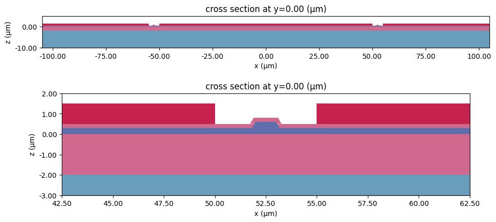
We can set up a test Scene to visualize the structures.
test_scene = td.Scene(medium=med_air, structures=structures_list_cpw_conventional)
# Plot the test scene
ypos = 0
fig, ax = plt.subplots(2, 1, figsize=(10, 5), tight_layout=True)
test_scene.plot(y=ypos, hlim=(-g - ws, g + ws), vlim=(-10, 5), ax=ax[0])
ax[0].set_aspect(1)
test_scene.plot(y=ypos, hlim=((g + ws) / 2 - 10, (g + ws) / 2 + 10), vlim=(-3, 2), ax=ax[1])
plt.show()
Grid and Boundary Conditions
The simulation domain is surrounded by Perfectly Matched Layers (PMLs) on all side by default. We add a quarter-wavelength padding on all sides to ensure that they do not encroach on the near-field.
# Define simulation size
padding = td.C_0 / f_max / 4
sim_LX = w_cpw + 2 * padding
sim_LY = sim_LX
sim_LZ = sim_LX
We make use of LayerRefinementSpec to refine the grid near the metallic CPW structures.
# Layer refinement around conductors
LR_spec_1 = rf.LayerRefinementSpec.from_structures(
    structures=str_cpw_conventional,
    min_steps_along_axis=5,
    refinement_inside_sim_only=False,
    corner_refinement=td.GridRefinement(dl=tm / 5, num_cells=2),
)
Additionally, we will also define a mesh refinement box around the optical waveguide for more accurate results.
# Mesh override structure around optical wavelength core
refine_box = td.MeshOverrideStructure(
    geometry=td.Box(center=((ws + g) / 2, 0, (tln1) / 2), size=(1.2 * w0, td.inf, (tln1))),
    dl=(w0 / 5.0, None, tln1 / 5.0),
)
The rest of the grid is automatically generated according to the wavelength.
# Define overall grid specification
grid_spec = td.GridSpec.auto(
    wavelength=td.C_0 / f_max,
    min_steps_per_wvl=12,
    override_structures=[refine_box],
    layer_refinement_specs=[LR_spec_1],
)
Wave Ports
Although we will not be running a 3D simulation in this section, we can nevertheless define a WavePort in order to facilitate the setup of the 2D mode analysis. The dummy wave port is defined below.
# Wave port dimensions
wp_center = (0, 0, 1)
wp_size = (w_cpw - 15, 0, w_cpw - 15)

# Define wave port
WP_dummy = rf.WavePort(
    center=wp_center,
    size=wp_size,
    mode_spec=rf.MicrowaveModeSpec(target_neff=np.sqrt(8)),
    direction="+",
    name="Dummy WP",
)
Mode Solver
As in the first notebook, we will conduct a 2D mode analysis to obtain key transmission line parameters.
# Define base mode solver simulation
ms_sim = td.Simulation(
    size=(sim_LX, sim_LY, sim_LZ),
    medium=med_air,
    grid_spec=grid_spec,
    structures=structures_list_cpw_conventional,
    symmetry=(1, 0, 0),
    run_time=1e-10,
)

# Define mode solver
mode_solver = WP_dummy.to_mode_solver(simulation=ms_sim, freqs=freqs)
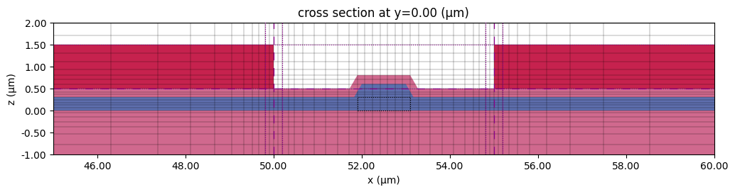
Before running, let us preview the transverse grid near the optical waveguide to ensure that it is suitably refined.
# Plot transverse grid
fig, ax = plt.subplots(figsize=(12, 4))
ms_sim.plot(y=0, ax=ax)
ms_sim.plot_grid(y=0, ax=ax, hlim=(ws / 2 - 5, ws / 2 + g + 5), vlim=(-1, 2))
plt.show()
We run the mode solver below.
mode_data = web.run(mode_solver, task_name="mode solver", path="data/mode_data.hdf5")
14:30:04 EST Created task 'mode solver' with resource_id
             'mo-b21460d3-498d-498b-a908-f41d864166e4' and task_type
             'MODE_SOLVER'.
             View task using web UI at
             'https://tidy3d.simulation.cloud/workbench?taskId=mo-b21460d3-498d-
             498b-a908-f41d864166e4'.
Task folder: 'default'.
Output()
14:30:06 EST Estimated FlexCredit cost: 0.016. Minimum cost depends on task
             execution details. Use 'web.real_cost(task_id)' to get the billed
             FlexCredit cost after a simulation run.
14:30:07 EST status = queued
             To cancel the simulation, use 'web.abort(task_id)' or
             'web.delete(task_id)' or abort/delete the task in the web UI.
             Terminating the Python script will not stop the job running on the
             cloud.
Output()
14:30:14 EST starting up solver
14:30:15 EST running solver
14:30:33 EST status = success
             View simulation result at
             'https://tidy3d.simulation.cloud/workbench?taskId=mo-b21460d3-498d-
             498b-a908-f41d864166e4'.
Output()
14:30:39 EST Loading simulation from data/mode_data.hdf5
2D Results
Mode Profile
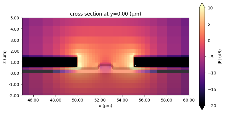
The field magnitude profile in one of the CPW gaps is shown below.
# Plot the mode field
fig, ax = plt.subplots(figsize=(8, 4), tight_layout=True)
mode_solver.plot_field(field_name="E", val="abs", scale="dB", f=40e9, ax=ax, vmax=10, vmin=-20)
ax.set_xlim(ws / 2 - 5, ws / 2 + g + 5)
ax.set_ylim(-2, 5)
plt.show()
/Library/Frameworks/Python.framework/Versions/3.13/lib/python3.13/site-packages/xarray/core/computation.py:824: RuntimeWarning: divide by zero encountered in log10
  result_data = func(*input_data)
/Library/Frameworks/Python.framework/Versions/3.13/lib/python3.13/site-packages/scipy/interpolate/_interpolate.py:482: RuntimeWarning: invalid value encountered in add
  y_new = slope*(x_new - x_lo)[:, None] + y_lo
Effective Index, Attenuation, and Characteristic Impedance
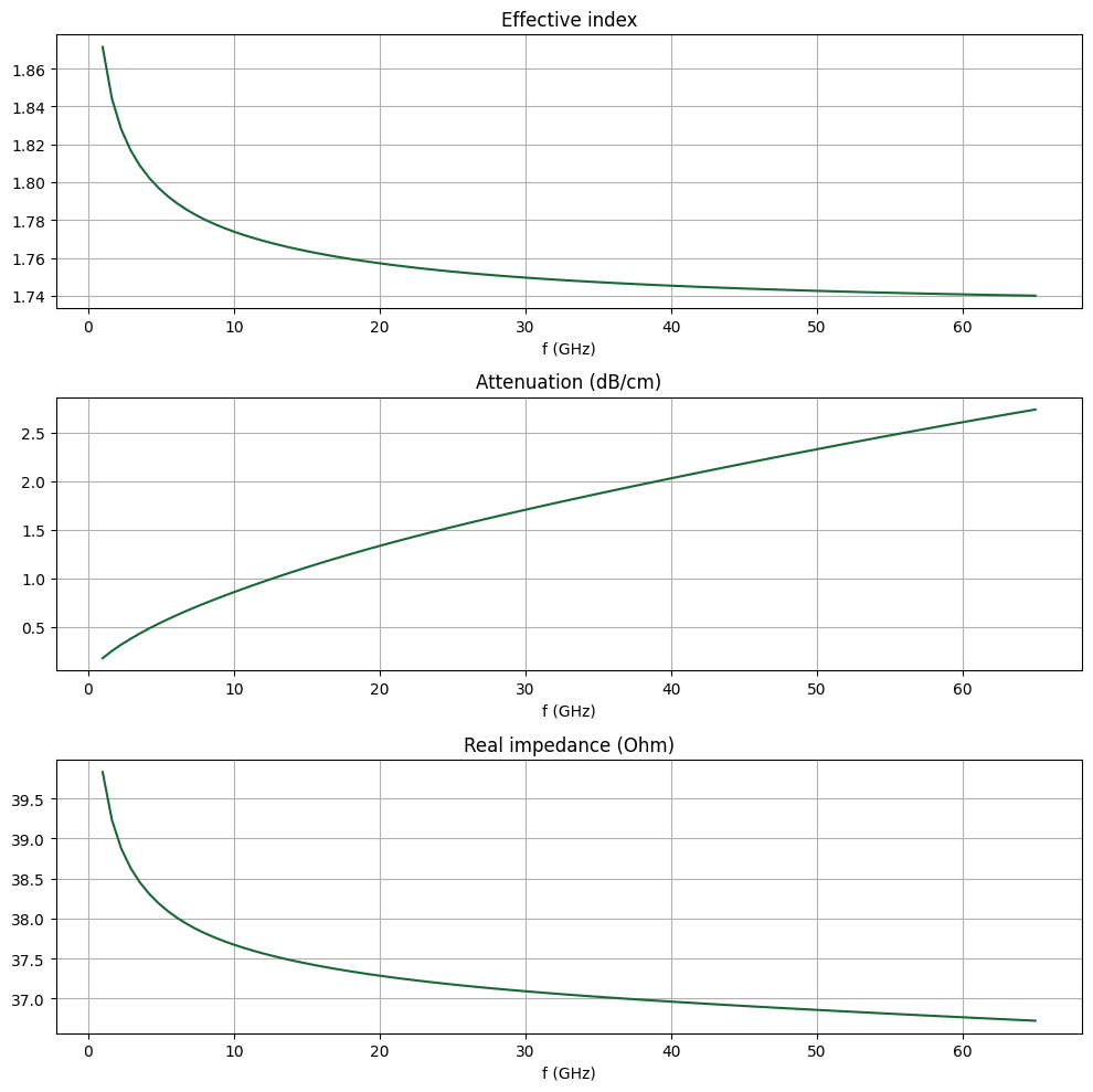
The key properties that determine a guided mode are effective index $n_\text{eff}$, attenuation $\alpha$, and characteristic impedance $Z_0$. We demonstrate how to obtain those values below.
We extract the first three quantities, $n_\text{eff}$, $\alpha$, and $\alpha$, directly from the mode solver data. Then, we use them to compute the complex propagation constant $\gamma = \beta + j\alpha$.
# Gather alpha, neff from mode solver results
neff_mode = mode_data.modes_info["n eff"].squeeze()
alphadB_mode = mode_data.modes_info["loss (dB/cm)"].squeeze()

# Get alpha, beta
alpha_mode = mode_data.alpha.isel(mode_index=0)
beta_mode = mode_data.beta.isel(mode_index=0)
# Gamma in 1/mm
gamma_mode = (alpha_mode + 1j * beta_mode) * 1e-3
The characteristic line impedance $Z_0$ is retrieved from the mode solver data as well. Note the use of np.conjugate() to convert from the physics phase convention (used in Tidy3D) to the standard electrical engineering phase convention.
# Retrieve the characteristic impedance from the mode impedance.
Z0_mode = np.conjugate(mode_data.transmission_line_data.Z0.isel(mode_index=0)).squeeze()
These values are plotted below.
fig, ax = plt.subplots(3, 1, figsize=(10, 10), tight_layout=True)
ax[0].set_title("Effective index")
ax[0].plot(freqs / 1e9, neff_mode)
ax[1].set_title("Attenuation (dB/cm)")
ax[1].plot(freqs / 1e9, alphadB_mode)
ax[2].set_title("Real impedance (Ohm)")
ax[2].plot(freqs / 1e9, np.real(Z0_mode))
for axis in ax:
    axis.grid()
    axis.set_xlabel("f (GHz)")
plt.show()
Distributed Transmission Line Parameters (RLCG)
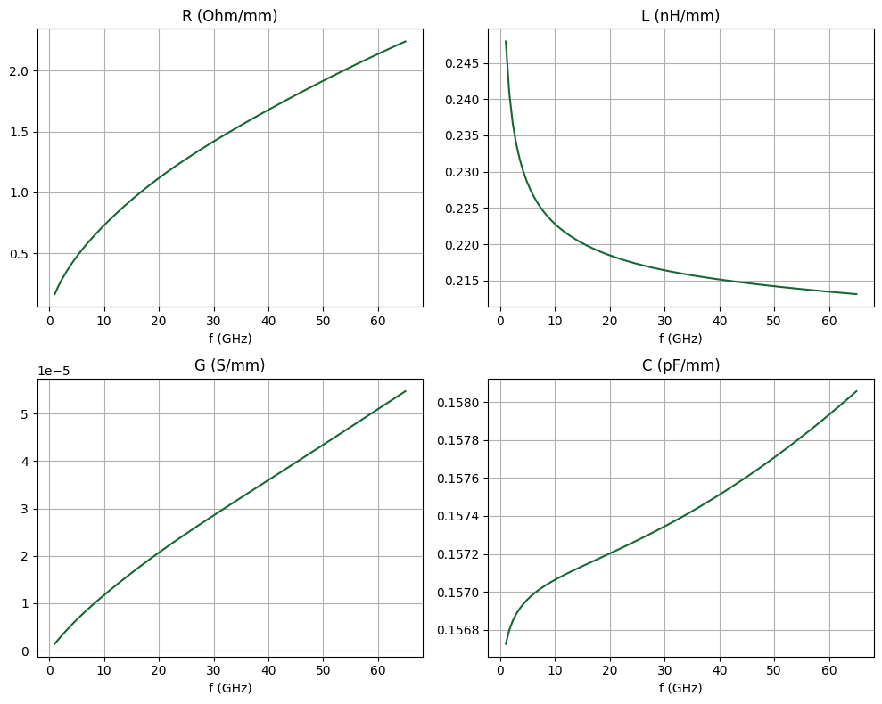
Using the complex propagation constant $\gamma$ and the line impedance $Z_0$, we can calculate the RLCG parameters using the following relationships: $$ R = \text{Re}(\gamma Z_0), \quad L = \text{Im}(\gamma Z_0)/\omega, \quad G = \text{Re}(\gamma/Z_0), \quad C = \text{Im}(\gamma/Z_0)/\omega $$ where $\omega = 2\pi f$.
R_mode = np.real(gamma_mode * Z0_mode)  # Ohm/mm
G_mode = np.real(gamma_mode / Z0_mode)  # S/mm
L_mode = np.imag(gamma_mode * Z0_mode) / (2 * np.pi * freqs)  # H/mm
C_mode = np.imag(gamma_mode / Z0_mode) / (2 * np.pi * freqs)  # F/mm
# Plot RLCG
fig, ax = plt.subplots(2, 2, figsize=(10, 8), tight_layout=False)
ax[0, 0].plot(freqs / 1e9, R_mode)
ax[0, 1].plot(freqs / 1e9, L_mode * 1e9)
ax[1, 0].plot(freqs / 1e9, G_mode)
ax[1, 1].plot(freqs / 1e9, C_mode * 1e12)
titles = ["R (Ohm/mm)", "L (nH/mm)", "G (S/mm)", "C (pF/mm)"]
for ii, title in enumerate(titles):
    ax[ii // 2, ii % 2].set_title(title)
    ax[ii // 2, ii % 2].set_xlabel("f (GHz)")
    ax[ii // 2, ii % 2].grid()
plt.show()
Segmented Electrodes (3D analysis)
Geometry
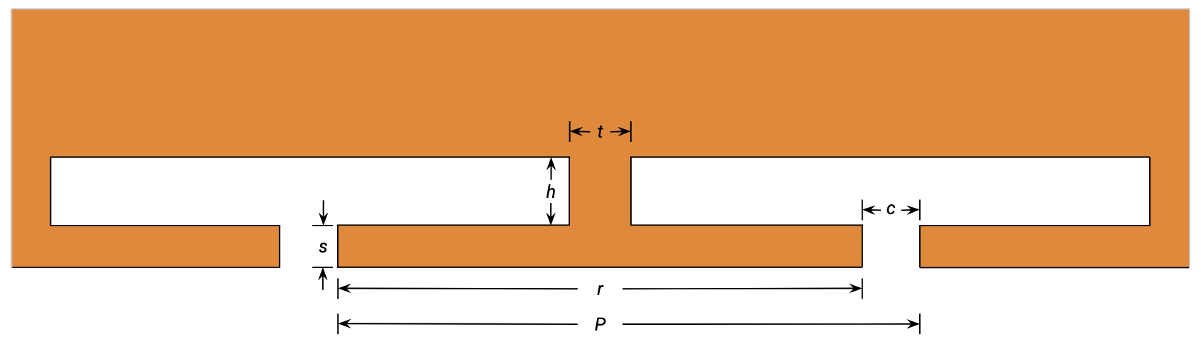
The T-electrode geometry parameters are defined below. The rest of the dimensions are identical to those defined previously. Because the segmented CPW is longitudinally inhomogeneous, we will be using short sections of conventional CPW on both ends to excite the structure.
# Define T-electrode dimensions
s, r = (2, 45)  # width and length, top of T
h, t = (6, 2)  # width and length, neck of T
c = 5  # gap between T units
P = r + c  # T electrode period
gw = g + 2 * (s + h)  # CPW gap including electrodes

# Define line lengths
LTL = 20 * P  # Length of segmented line
Lin = 5 * P  # CPW length, input section
Lout = 5 * P  # CPW length, output section
We make use of parameterized functions to create the T-electrode and segmented CPW.
def create_T_structure(base_position, direction, width_r, width_t, width_s, width_h):
    """Create a T-shaped electrode"""
    x0, y0 = base_position
    sgn = 1 if direction == "+" else -1

    geom_T = [
        td.Box(
            size=(width_s, width_r, tm),
            center=(x0 + sgn * (width_h + width_s / 2), y0, tln0 - tln1 + tsio21 + tm / 2.0),
        ),
        td.Box(
            size=(width_h, width_t, tm),
            center=(x0 + sgn * width_h / 2, y0, tln0 - tln1 + tsio21 + tm / 2.0),
        ),
    ]

    return geom_T
def create_segmented_cpw(r, t, s, h, g, ws, P, L):
    """Creates segmented CPW and optical waveguide core/cladding"""
    gw = g + 2 * (s + h)  # CPW gap including electrodes

    # Optical WG Core + Cladding
    wg_core = create_rib_structure(
        w0, tln0 - tln1, thetaln, ((ws + gw) / 2, tln0 - tln1 / 2.0), med_LN
    )
    wg_clad = create_rib_structure(
        1.2 * w0, tln0 - tln1, thetaln, ((ws + gw) / 2, tln0 - tln1 / 2.0 + tsio21), med_SiO2
    )

    # Wide CPW in segmented section
    cpw_list_wide = create_cpw(gw, ws, wg - (s + h), tm, -len_inf, len_inf)

    # Narrow CPW for input/output section
    cpw_list_narrow = create_cpw(g, ws + 2 * (s + h), wg, tm, -len_inf, -L / 2) + create_cpw(
        g, ws + 2 * (s + h), wg, tm, L / 2, len_inf
    )

    # T-segments
    num_units = int(L / P)
    T_geom_list = []
    for ii in range(num_units + 1):
        xx0, xx1, xx2, xx3 = (-ws / 2 - gw, -ws / 2, ws / 2, ws / 2 + gw)
        yy = -P * num_units / 2 + (ii) * P
        T_geom_list += create_T_structure((xx0, yy), "+", r, t, s, h)
        T_geom_list += create_T_structure((xx1, yy), "-", r, t, s, h)
        T_geom_list += create_T_structure((xx2, yy), "+", r, t, s, h)
        T_geom_list += create_T_structure((xx3, yy), "-", r, t, s, h)
    T_structure = td.Structure(medium=med_Au, geometry=td.GeometryGroup(geometries=T_geom_list))

    return [wg_core, wg_clad, T_structure] + cpw_list_wide + cpw_list_narrow


# Create segmented CPW
structures_cpw_segmented = create_segmented_cpw(r, t, s, h, g, ws, P, LTL)

# Combine list of structures
structures_list_cpw_segmented = structures_layers + structures_cpw_segmented
Grid and Boundary
The simulation size is defined below.
# Simulation dimensions
sim_size = (sim_LX, LTL + Lin + Lout, sim_LZ)
sim_center = (0, -(Lin - Lout) / 2, 0)
We use the same grid refinement strategy as before. For 3D simulation, usually a lower level of refinement is necessary to achieve converged S-parameter results.
# Layer refinement around conductors
LR_spec_2 = rf.LayerRefinementSpec(
    center=(0, 0, 1),
    size=(td.inf, td.inf, 1),
    axis=2,
    corner_refinement=td.GridRefinement(dl=tm, num_cells=2),
    refinement_inside_sim_only=False,
)

refine_box_2 = td.MeshOverrideStructure(
    geometry=td.Box(center=((ws + gw) / 2, 0, (tln1) / 2), size=(1.2 * w0, td.inf, (tln1))),
    dl=(w0 / 5.0, None, tln0 / 2),
)
# Define grid spec
grid_spec_2 = td.GridSpec.auto(
    wavelength=td.C_0 / f_max,
    min_steps_per_wvl=20,
    override_structures=[refine_box_2],
    layer_refinement_specs=[LR_spec_2],
)
Wave Ports and Monitors
The two wave ports are positioned along the input and output sections of the conventional CPW with a 100 micron spacing to the segmented structure.
wp_offset = 100  # wave port offset

# Define wave ports
WP1 = rf.WavePort(
    name="WP1",
    center=(0, -LTL / 2 - wp_offset, 1),
    size=wp_size,
    mode_spec=rf.MicrowaveModeSpec(target_neff=np.sqrt(8)),
    direction="+",
)
WP2 = WP1.updated_copy(
    name="WP2",
    center=(0, LTL / 2 + wp_offset, 0),
    direction="-",
)
We define a field monitor for visualization purposes.
# Define monitors
mon_field1 = td.FieldMonitor(
    center=(0, 0, 1),
    size=(w_cpw, len_inf, 0),
    freqs=[f_min, f0, f_max],
    name="field cpw plane",
)

monitors_list = [mon_field1]
Define Simulation and TerminalComponentModeler
# Define base simulation
sim = td.Simulation(
    center=sim_center,
    size=sim_size,
    grid_spec=grid_spec_2,
    structures=structures_list_cpw_segmented,
    monitors=monitors_list,
    run_time=2e-10,
    symmetry=(1, 0, 0),
)
# Define TerminalComponentModeler
tcm = rf.TerminalComponentModeler(
    simulation=sim,
    ports=[WP1, WP2],
    freqs=freqs,
)
Visualization
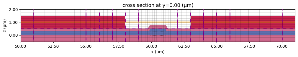
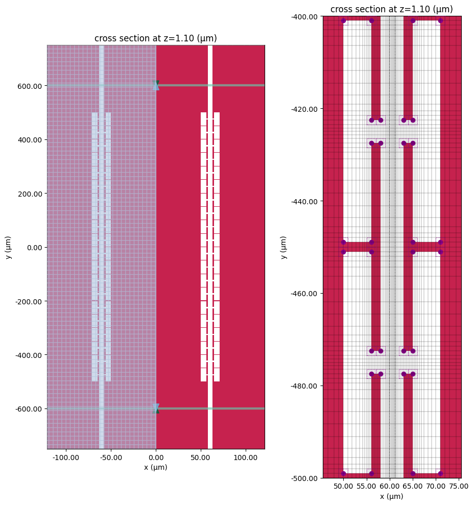
We plot the transverse and longitudinal cross sections to check that the structures and grid are properly set up.
# Plot structure/grid in CPW gap
fig, ax = plt.subplots(figsize=(12, 4))
sim.plot(y=0, ax=ax)
sim.plot_grid(y=0, ax=ax, hlim=(ws / 2, ws / 2 + gw), vlim=(-0.5, 2))
plt.show()
# Plot structure/grid in metal plane
fig, ax = plt.subplots(1, 2, figsize=(10, 10), tight_layout=True)
tcm.plot_sim(
    z=1.1,
    ax=ax[0],
    hlim=(-gw - ws, gw + ws),
    vlim=(-LTL / 2 - Lin, LTL / 2 + Lout),
)
# sim.plot_grid(z=1.1, hlim=(-gw-ws, gw+ws), vlim=(-LTL/2-Lin,LTL/2+Lout), ax=ax[0])
ax[0].set_aspect(0.3)

tcm.plot_sim(z=1.1, ax=ax[1])
sim.plot_grid(
    z=1.1,
    hlim=((gw + ws) / 2 - 15, (gw + ws) / 2 + 15),
    vlim=(-LTL / 2, -LTL / 2 + 2 * P),
    ax=ax[1],
)
plt.show()
Run Simulation
tcm_data = web.run(tcm, task_name="segmented cpw", path="data/segmented_cpw.hdf5")
14:30:42 EST Created task 'segmented cpw' with resource_id
             'sid-5962ca38-c2c7-4b23-af3e-818b27fae3ed' and task_type
             'TERMINAL_CM'.
             View task using web UI at
             'https://tidy3d.simulation.cloud/rf?taskId=pa-e08bc6bd-d53b-4d18-8e
             59-59fd08de4ad2'.
Task folder: 'default'.
Output()
14:30:54 EST Maximum FlexCredit cost: 5.925. Minimum cost depends on task
             execution details. Use 'web.real_cost(task_id)' after run.
14:30:55 EST Subtasks status - segmented cpw
             Group ID: 'pa-e08bc6bd-d53b-4d18-8e59-59fd08de4ad2'
Output()
Batch status = preprocess
14:31:02 EST Batch status = running
14:38:12 EST Batch status = postprocess
14:38:40 EST Modeler has finished running successfully.
14:38:41 EST Billed flex credit cost: 3.588.
Output()
14:39:00 EST Loading component modeler data from data/segmented_cpw.hdf5
Results
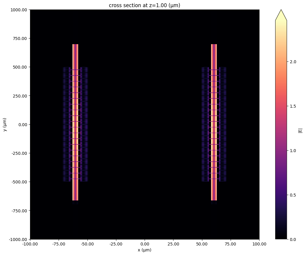
Field Profile
First, let us take a look at the field monitor data. The field magnitude in the CPW gap is shown below.
# Load simulation data from TCM data
sim_data = tcm_data.data["WP1@0"]

# longitudinal field
fig, ax = plt.subplots(figsize=(14, 10))
f_plot = f_max
sim_data.plot_field("field cpw plane", field_name="E", val="abs", ax=ax, f=f_plot)
ax.set_xlim(-100, 100)
ax.set_ylim(-1000, 1000)
ax.set_aspect(0.1)
plt.show()
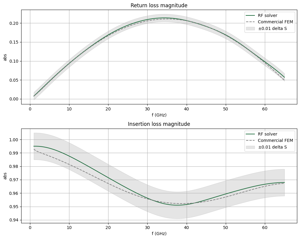
S-parameters
The S-matrix can be calculated using the smatrix() method. We also define several convenience functions to get a specific S_ij in different formats.
# Calculate S-matrix dataset
smat = tcm_data.smatrix()


# Convenience functions
def sparam(i, j):
    return np.conjugate(smat.data.isel(port_in=j - 1, port_out=i - 1))


def sparam_abs(i, j):
    return np.abs(sparam(i, j))


def sparam_dB(i, j):
    return 20 * np.log10(sparam_abs(i, j))
For comparison purposes, we import benchmark data from a commercial FEM solver.
# Import benchmark data
freqs_ben, S21abs_ben, S11abs_ben = np.genfromtxt(
    "misc/seg_fem_sparam.csv", skip_header=1, delimiter=",", unpack=True
)
The return and insertion loss magnitudes are compared below. We find a good overall match. We also note a considerable speed improvement using the Tidy3D RF solver (approx. 3.5 minutes) versus conventional FEM (approx. 1.5 hours).
fig, ax = plt.subplots(2, 1, figsize=(10, 8), tight_layout=True)
delta_S = 0.01
ax[0].set_title("Return loss magnitude")
ax[0].plot(freqs / 1e9, sparam_abs(1, 1), label="RF solver")
ax[0].plot(freqs_ben, S11abs_ben, "--", color="gray", label="Commercial FEM")
ax[0].fill_between(
    freqs / 1e9,
    sparam_abs(1, 1) - delta_S,
    sparam_abs(1, 1) + delta_S,
    color="gray",
    alpha=0.2,
    label="$\\pm$0.01 delta S",
)

ax[1].set_title("Insertion loss magnitude")
ax[1].plot(freqs / 1e9, sparam_abs(2, 1), label="RF solver")
ax[1].plot(freqs_ben, S21abs_ben, "--", color="gray", label="Commercial FEM")
ax[1].fill_between(
    freqs / 1e9,
    sparam_abs(2, 1) - delta_S,
    sparam_abs(2, 1) + delta_S,
    color="gray",
    alpha=0.2,
    label="$\\pm$0.01 delta S",
)
for axis in ax:
    axis.legend()
    axis.grid()
    axis.set_xlabel("f (GHz)")
    axis.set_ylabel("abs")
plt.show()
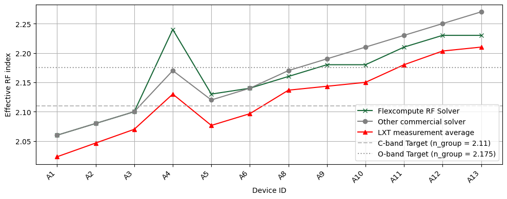
Experimental verification of TFLT segmented CPW with Luxtelligence SA
In collaboration with Luxtelligence SA (LXT), we used the RF solver to simulate a range of segmented electrode designs in their thin-film lithium tantalate (TFLT) platform. The results were compared against measurements and simulations on other commercial software performed by LXT.
Compared to lithium niobate, thin-film lithium tantalate offers a five-fold improvement in hour-scale bias stability, supports modulation down to tens of hertz, exhibits approximately twenty-times lower birefringence, provides nearly double the optical power damage threshold, and features a larger bandgap. Together, these properties make thin-film lithium tantalate a very promising platform for advanced telecommunication and datacom components, such as arrayed waveguide gratings (AWGs); enable dispersion engineering for optical-comb generation; and support high-performance frequency-metrology systems, as well as quantum applications operating across the visible-to-telecom wavelength range.
In a separate Tidy3D mode solver simulation, the group index of the fundamental TE mode of the TFLT ridge waveguide (based on the ltoi300 PDK of LXT) was calculated. The waveguide has dimensions given by a total height of 300 nm, slab thickness of 120 nm, and ridge width of 2.5 um. The simulations were performed at 1550 nm (C-band) and 1310 nm (O-band), and the group index was calculated to be 2.11 and 2.175 respectively. For more information about the stack, please contact Luxtelligence SA.
The high-frequency RF effective index should match the optical group index to enable high-speed data transmission. We performed a sweep of 12 T-rail designs from LXT (A1-A13) and sought to match the effective index at the RF frequency of 67 GHz. The results are presented below alongside actual measurement data from LXT. Additionally, results from a similar calculation performed by LXT using a different commercial EM solver are also included.
# Import LXT data
_, neff_lxt_tidy3d, neff_lxt_comm, neff_lxt_exp = np.genfromtxt(
    "misc/cpw_lxt_data.csv", skip_header=1, delimiter=",", unpack=True
)
device_labels = ["A1", "A2", "A3", "A4", "A5", "A6", "A8", "A9", "A10", "A11", "A12", "A13"]

# Create comparison plot
fig, ax = plt.subplots(figsize=(10, 4), tight_layout=True)
ax.plot(neff_lxt_tidy3d, "-x", label="Flexcompute RF Solver")
ax.plot(neff_lxt_comm, "-o", color="gray", label="Other commercial solver")
ax.plot(neff_lxt_exp, "-^", color="red", label="LXT measurement average")
ax.axhline(2.11, ls="--", color="#bbbbbb", label="C-band Target (n_group = 2.11)")
ax.axhline(2.175, ls=":", color="#999999", label="O-band Target (n_group = 2.175)")

ax.set_ylabel("Effective RF index")
ax.set_xlabel("Device ID")
ax.set_xticks(np.arange(0, 12, 1))
ax.set_xticklabels(device_labels, rotation=45, ha="right")
ax.grid()
ax.legend()
plt.show()
Conclusion
In this notebook, we studied the CPW in the context of a Mach-Zehnder modulator. We simulated two different configurations, namely the conventional straight CPW and segmented electrodes design, and obtained key transmission line parameters. Additionally, we also performed experimental verification of the RF solver using designs and measurement data from LXT.