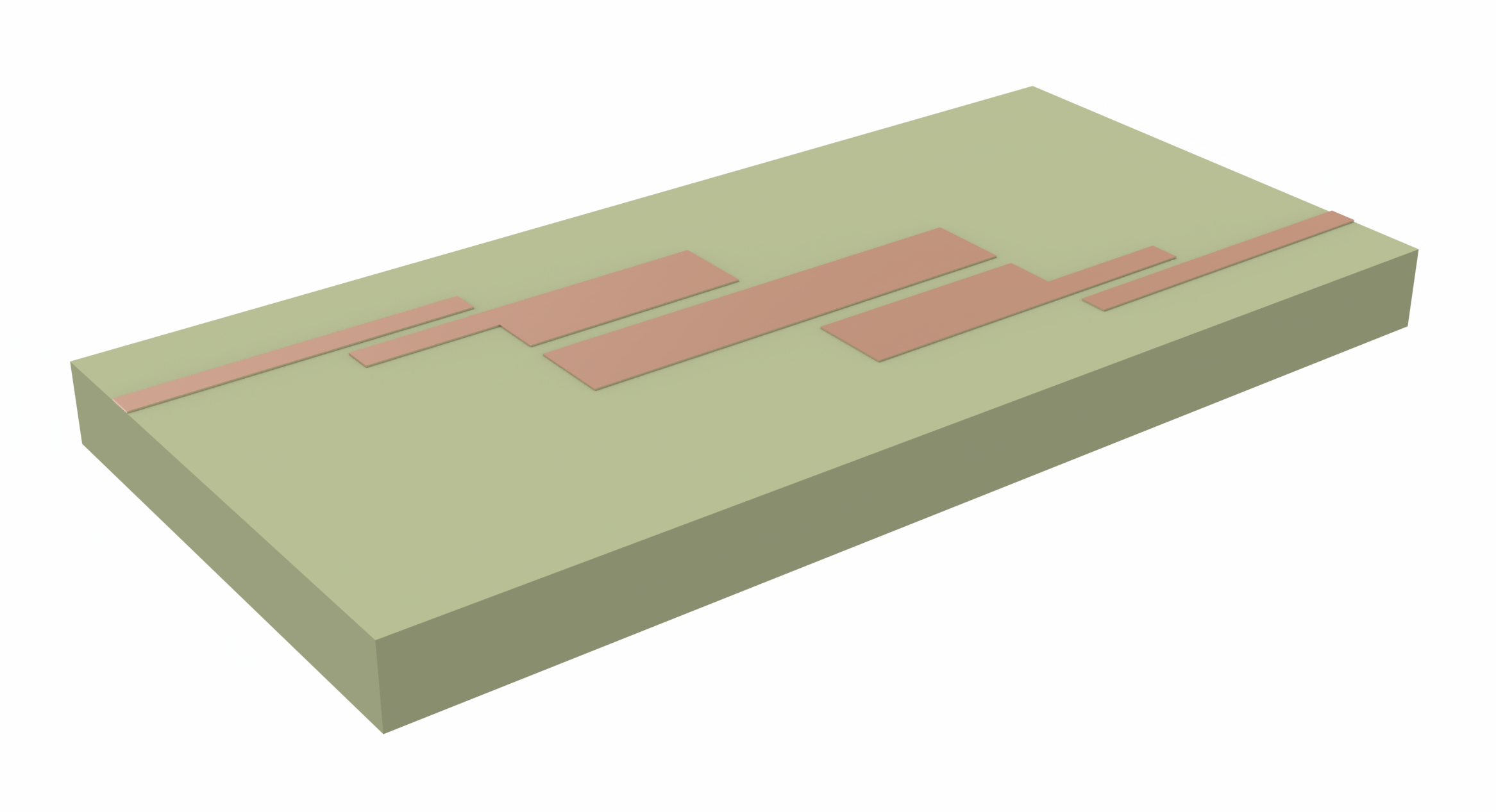
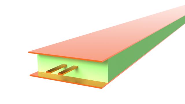
The stripline is a commonly used transmission line in printed circuit board (PCB) designs. Compared to the microstrip, the advantage of the stripline includes better shielding from EM interference, lower radiation loss, and better performance at higher frequencies. These strengths make it suitable for use in high-speed interconnects, where bandwidth, package size, and signal integrity are key concerns.
In this notebook, we will build a 100 Ohm edge-coupled differential stripline and simulate it from 1 to 70 GHz. The results will be compared with benchmark data from other commercial RF simulation software. Both 2D mode solver and 3D FDTD results are presented.
import matplotlib.pyplot as plt
import numpy as np
import tidy3d as td
import tidy3d.rf as rf
import tidy3d.web as web
from tidy3d.plugins.dispersion import FastDispersionFitter

td.config.logging.level = "ERROR"
Building the Simulation
Key Parameters
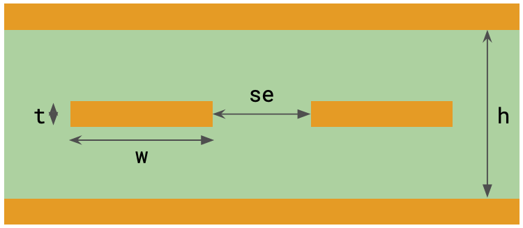
We begin by defining some key parameters. The design impedance $Z_0$ for the differential mode will be 100 Ohms. The geometry parameters are chosen with that in mind. Material properties are assumed constant over the frequency band.
# Frequency range (Hz)
f_min, f_max = (1e9, 70e9)

# Center frequency
f0 = (f_max + f_min) / 2

# Frequency sample points
freqs = np.linspace(f_min, f_max, 101)

# Frequency sample points (for field monitors)
field_mon_freqs = np.linspace(f_min, f_max, 3)
# Geometry
mil = 25.4  # conversion to mils to microns (default unit)
w = 3.2 * mil  # Signal strip width
t = 0.7 * mil  # Conductor thickness
h = 10.7 * mil  # Substrate thickness
se = 7 * mil  # gap between edge-coupled pair
L = 4000 * mil  # Line length
len_inf = 1e6  # Effective infinity
# Material properties
cond = 60  # Metal conductivity in S/um
eps = 4.4  # Relative permittivity, substrate
losstan = 0.0012  # Loss tangent, substrate
Mediums and Structures
We wish to define constant loss for the metal and substrate over the frequency band:
- Metal: The
LossyMetalMediumimplements the surface impedance boundary condition for lossy metals . - Dielectric: The
constant_loss_tangent_modelmethod in theFastDispersionFitterplugin automatically generates aPoleResiduemedium given permittivity, loss tangent, and frequency range parameters.
med_sub = FastDispersionFitter.constant_loss_tangent_model(
    eps, losstan, (f_min, f_max), tolerance_rms=2e-4
)
med_metal = rf.LossyMetalMedium(conductivity=cond, frequency_range=(f_min, f_max), name="Metal")
We can also use VisualizationSpec to control the fill color of the materials during plotting.
med_sub = med_sub.updated_copy(
    viz_spec=td.VisualizationSpec(facecolor="#7cc48d")
)  # green tone for substrate
med_metal = med_metal.updated_copy(
    viz_spec=td.VisualizationSpec(facecolor="#ed8026")
)  # copper tone for metal
The structures are created below.
# Substrate
str_sub = td.Structure(
    geometry=td.Box(center=(0, 0, 0), size=(len_inf, h, len_inf)), medium=med_sub
)

# Left signal strip
str_strip_left = td.Structure(
    geometry=td.Box(center=(-(se + w) / 2, 0, 0), size=(w, t, len_inf)), medium=med_metal
)

# Right signal strip
str_strip_right = td.Structure(
    geometry=td.Box(center=((se + w) / 2, 0, 0), size=(w, t, len_inf)), medium=med_metal
)

# Top ground plane
str_gnd_top = td.Structure(
    geometry=td.Box(center=(0, h / 2 + t / 2, 0), size=(len_inf, t, len_inf)), medium=med_metal
)

# Bottom ground plane
str_gnd_bot = td.Structure(
    geometry=td.Box(center=(0, -h / 2 - t / 2, 0), size=(len_inf, t, len_inf)), medium=med_metal
)
Grid and Boundaries
The LayerRefinementSpec feature is useful for refining the grid around metallic structures as it automatically detects metal edges and corners. In this model, we define lr_spec in order to refine the region around the left and right signal traces. The other specs lr_spec2 and lr_spec3 are used to refine the region around the top and bottom ground planes.
# Create a LayerRefinementSpec from signal trace structures
lr_spec = rf.LayerRefinementSpec.from_structures(
    structures=[str_strip_left, str_strip_right],
    axis=1,  # Layer normal is in y-direction
    min_steps_along_axis=10,  # Min 10 grid cells along normal direction
    refinement_inside_sim_only=False,  # Metal structures extend outside sim domain. Set 'False' to snap to corners outside sim.
    bounds_snapping="bounds",  # snap grid to metal boundaries
    corner_refinement=td.GridRefinement(
        dl=t / 10, num_cells=2
    ),  # snap to corners and apply added refinement
)

# Layer refinement for top and bottom ground planes
lr_spec2 = lr_spec.updated_copy(center=(0, h / 2 + t / 2, 0), size=(len_inf, t, len_inf))
lr_spec3 = lr_spec.updated_copy(center=(0, -h / 2 - t / 2, 0), size=(len_inf, t, len_inf))
The rest of the grid is automatically generated based on the wavelength.
# Define overall grid specification
grid_spec = td.GridSpec.auto(
    wavelength=td.C_0 / f_max,
    min_steps_per_wvl=30,
    layer_refinement_specs=[lr_spec, lr_spec2, lr_spec3],
)
The top and bottom boundaries of this model are adjacent to the metal ground planes and can be set to PEC. All other boundaries are open and thus truncated by perfectly matched layers (PMLs).
boundary_spec = td.BoundarySpec(
    x=td.Boundary.pml(),
    y=td.Boundary.pec(),
    z=td.Boundary.pml(),
)
Monitors
For visualization purposes, we will add a FieldMonitor along the longitudinal plane.
field_mon_1 = td.FieldMonitor(
    center=(0, 0, 0),
    size=(len_inf, 0, len_inf),
    freqs=field_mon_freqs,
    name="longitudinal field (y=0)",
)
Wave Ports
Wave ports are used to excite the model and calculate S-parameters. In addition to the name, center, size, and orientation direction, the wave port also requires defining:
- The
mode_specsetting, which controls the specification for the wave port mode solver. Typically, we solve for one mode with thetarget_neffclose to the expected propagation index. - By default the
MicrowaveModeSpecis setup to automatically compute impedance for modes using anAutoImpedanceSpec. Alternatively, you may use aCustomImpedanceSpecwhich requires either avoltage_spec, orcurrent_spec, or both. These definitions are used to calculate the mode's characteristic impedance $Z_0$. Note that depending on which integral is specified, there are three possible conventions: PI, PV, or VI where P = power, V = voltage, I = current. Each convention will yield a slightly different value for the impedance. In this notebook, we use the VI convention. TheAutoImpedanceSpecuses the PI convention for computing impedance.
# Define current and voltage integral specifications
current_spec = rf.AxisAlignedCurrentIntegralSpec(
    center=((se + w) / 2, 0, -L / 2), size=(2 * w, 3 * t, 0), sign="+"
)
voltage_spec = rf.AxisAlignedVoltageIntegralSpec(
    center=(0, 0, -L / 2),
    size=(se, 0, 0),
    extrapolate_to_endpoints=True,
    snap_path_to_grid=True,
    sign="+",
)
# Define specification for computing characteristic impedance
Z_VI_impedance_spec = rf.CustomImpedanceSpec(voltage_spec=voltage_spec, current_spec=current_spec)
# Define port specification
wave_port_mode_spec = rf.MicrowaveModeSpec(
    num_modes=1, target_neff=np.sqrt(eps), impedance_specs=(Z_VI_impedance_spec,)
)

# Define wave ports
WP1 = rf.WavePort(
    center=(0, 0, -L / 2),
    size=(len_inf, len_inf, 0),
    mode_spec=wave_port_mode_spec,
    direction="+",
    name="WP1",
)
# Update the mode spec for the second wave port. We only need to update the sign of the current specification, since coordinates along
# the longitudinal direction are ignored, and the ports are identical in the transverse plane.
wave_port_mode_spec = wave_port_mode_spec.updated_copy(
    path="impedance_specs/0/", current_spec=current_spec.updated_copy(sign="-")
)
WP2 = WP1.updated_copy(
    name="WP2",
    center=(0, 0, L / 2),
    direction="-",
    mode_spec=wave_port_mode_spec,
)
Define the Simulation and TerminalComponentModeler
The Simulation object in Tidy3D contains information about the entire simulation environment, including boundary conditions, grid, structures, and monitors.
sim = td.Simulation(
    size=(50 * mil, h + 2 * t, 1.05 * L),
    center=(0, 0, 0),
    grid_spec=grid_spec,
    boundary_spec=boundary_spec,
    structures=[str_sub, str_strip_left, str_strip_right, str_gnd_top, str_gnd_bot],
    monitors=[field_mon_1],
    run_time=2e-9,  # simulation run time in seconds
    shutoff=1e-7,  # lower shutoff threshold for more accurate small signal
    plot_length_units="mm",
    symmetry=(-1, 0, 0),  # odd symmetry in x-direction
)
The TerminalComponentModeler conducts a port sweep based on our previously defined Simulation in order to construct the full S-parameter matrix.
tcm = rf.TerminalComponentModeler(
    simulation=sim,  # simulation, previously defined
    ports=[WP1, WP2],  # wave ports, previously defined
    freqs=freqs,  # S-parameter frequency points
)
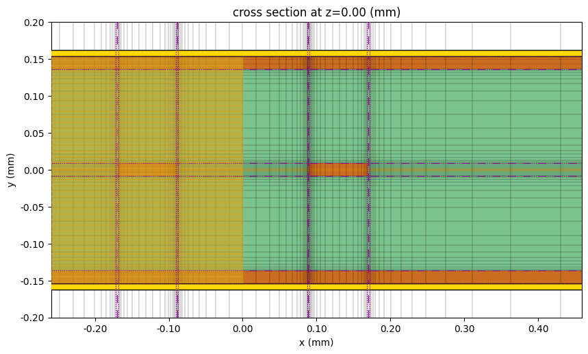
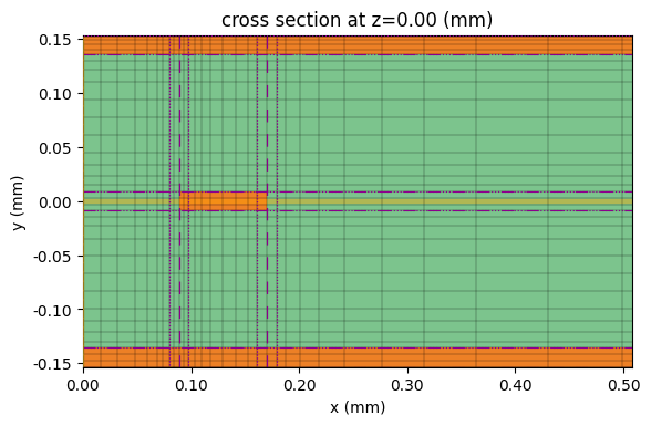
Before running, it is a good idea to double check the structures and grid. We see the substrate in green, and lossy metal in orange. The PEC top/bottom boundaries are displayed in gold.
# Inspect transverse grid
fig, ax = plt.subplots(figsize=(10, 6))
sim.plot(z=1, ax=ax)
sim.plot_grid(z=1, ax=ax, hlim=(-w - se, w + se + 200), vlim=(-200, 200))
plt.show()
2D Analysis
Before running the 3D simulation, let us first perform a 2D ModeSolver calculation. From the ModeSolver results, we can obtain all the key transmission line parameters, such as attenuation $\alpha$, characteristic impedance $Z_0$, and effective index $n_{\text{eff}}$.
Since we have previously defined a WavePort, we can skip the usual setup process and use the to_mode_solver() method to quickly define a ModeSolver simulation.
# Convert wave port to mode solver
mode_solver = WP1.to_mode_solver(sim, freqs)
We execute the mode solver study below.
mode_data = td.web.run(mode_solver, task_name="mode solver")
17:41:34 EST Created task 'mode solver' with resource_id
             'mo-07340d73-0320-4a69-a9a7-60328363d77b' and task_type
             'MODE_SOLVER'.
             View task using web UI at
             'https://tidy3d.simulation.cloud/workbench?taskId=mo-07340d73-0320-
             4a69-a9a7-60328363d77b'.
Task folder: 'default'.
17:41:42 EST Estimated FlexCredit cost: 0.014. Minimum cost depends on task
             execution details. Use 'web.real_cost(task_id)' to get the billed
             FlexCredit cost after a simulation run.
17:41:43 EST status = queued
             To cancel the simulation, use 'web.abort(task_id)' or
             'web.delete(task_id)' or abort/delete the task in the web UI.
             Terminating the Python script will not stop the job running on the
             cloud.
17:41:55 EST starting up solver
running solver
17:42:02 EST status = success
             View simulation result at
             'https://tidy3d.simulation.cloud/workbench?taskId=mo-07340d73-0320-
             4a69-a9a7-60328363d77b'.
17:42:05 EST Loading simulation from simulation_data.hdf5
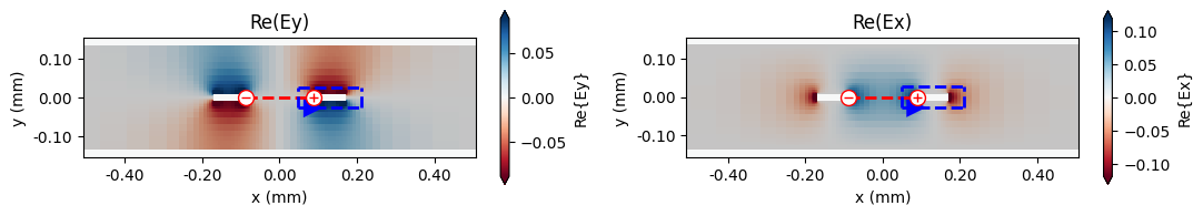
Below, the Ey and Ex components of the mode field are plotted at the center frequency. The integration paths for the impedance calculation are also shown (current in blue and voltage in red).
# Plot mode field
fig, ax = plt.subplots(1, 2, figsize=(11, 2), tight_layout=True)
mode_solver.plot_field(field_name="Ey", val="real", mode_index=0, f=f0, ax=ax[0])
mode_solver.plot_field(field_name="Ex", val="real", mode_index=0, f=f0, ax=ax[1])
for axis in ax:
    current_spec.plot(z=-L / 2, ax=axis)
    voltage_spec.plot(z=-L / 2, ax=axis)
    axis.set_xlim(-20 * mil, 20 * mil)
ax[0].set_title("Re(Ey)")
ax[1].set_title("Re(Ex)")
plt.show()
The mode solver solution data includes $n_{\text{eff}}$ and attenuation $\alpha$ in dB/cm. From this, we can also derive the real part of the propagation constant, $\beta$, as well as the complex propagation constant $\gamma$.
mode_data: td.MicrowaveModeSolverData = mode_data
# Gather alpha, neff from mode solver results
neff_mode = mode_data.modes_info["n eff"].squeeze()
alphadB_mode = mode_data.modes_info["loss (dB/cm)"].squeeze()

# Retrieve beta (rad/m), alpha (in Np/m), and gamma
beta_mode = mode_data.beta
alpha_mode = mode_data.alpha
gamma_mode = mode_data.gamma
We obtain $Z_0$ by accessing the Z0 field in the TransmissionLineDataset, making use of the previously defined current and voltage specifications.
Z0_mode = mode_data.transmission_line_data.Z0.isel(mode_index=0)
Let's import some benchmark data for comparison. We will use mode data from a commercial FEM and FIT solver respectively.
# Import benchmark data
freqs_ben1, neff_ben1, alphadB_ben1, Z0_ben1 = np.loadtxt(
    "./misc/stripline_fem_mode.csv", delimiter=",", skiprows=1, unpack=True
)
freqs_ben2, neff_ben2, alphadB_ben2, Z0_ben2 = np.loadtxt(
    "./misc/stripline_fit_mode.txt", delimiter=",", unpack=True
)
Let's compare the effective index $n_{\text{eff}}$.
def plot_data_and_band(data, err_band, ax, label=""):
    """Plots frequency-domain data together with a fractional error band"""
    ax.plot(freqs / 1e9, data, label=label, color="#328362")
    ax.fill_between(
        freqs / 1e9,
        (1 + err_band) * data,
        (1 - err_band) * data,
        alpha=0.5,
        color="#DDDDDD",
        label=f"+/-{err_band * 100:.2f}%",
    )
    ax.legend()
fig, ax = plt.subplots(figsize=(8, 4), tight_layout=True)
plot_data_and_band(neff_mode, 0.002, ax=ax, label="RF Photonics solver (Flexcompute)")
ax.plot(freqs_ben1, neff_ben1, "--", color="#888888", label="Commercial FEM")
ax.plot(freqs_ben2, neff_ben2, ":", color="#888888", label="Commercial FIT")
ax.set_title("Effective index")
ax.set_xlabel("f (GHz)")
ax.set_ylabel("$n_{\\text{eff}}$")
ax.set_ylim(2.09, 2.14)
ax.legend()
plt.show()
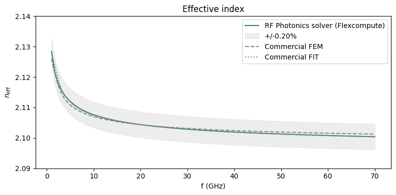
We observe that $n_{\text{eff}}$ is in good agreement with the benchmarks, and is close to the substrate index $\sqrt \epsilon \approx 2.10$.
Next, let's compare the transmission line losses $\alpha$ (dB/cm).
fig, ax = plt.subplots(figsize=(8, 4), tight_layout=True)
plot_data_and_band(alphadB_mode, 0.05, ax=ax, label="RF Photonics solver (Flexcompute)")
ax.plot(freqs_ben1, alphadB_ben1, "--", color="#888888", label="Commercial FEM")
ax.plot(freqs_ben2, alphadB_ben2, ":", color="#888888", label="Commercial FIT")
ax.set_title("Attenuation")
ax.set_xlabel("f (GHz)")
ax.set_ylabel("$\\alpha$ (dB/cm)")
ax.legend()
plt.show()
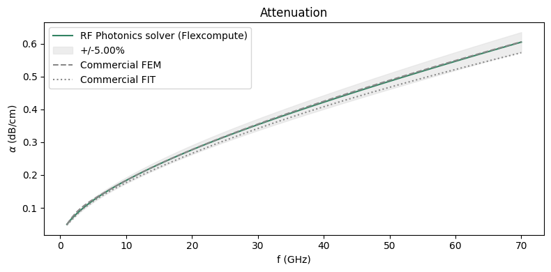
Although the metal and substrate mediums are both lossy in this simulation, the metal losses dominate in this frequency range and scale as $f^{1/2}$ due to the skin depth.
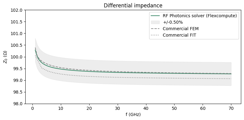
Let's compare the impedance $Z_0$ of the differential mode.
fig, ax = plt.subplots(figsize=(8, 4), tight_layout=True)
plot_data_and_band(np.real(Z0_mode), 0.005, ax=ax, label="RF Photonics solver (Flexcompute)")
ax.plot(freqs_ben1, Z0_ben1, "--", color="#888888", label="Commercial FEM")
ax.plot(freqs_ben2, Z0_ben2, ":", color="#888888", label="Commercial FIT")
ax.set_title("Differential impedance")
ax.set_xlabel("f (GHz)")
ax.set_ylabel("$Z_0$ ($\\Omega$)")
ax.set_ylim(98, 102)
ax.legend()
plt.show()
3D Analysis
Since the transmission line is longitudinally invariant, the results of the 2D analysis can fully describe the propagating TEM mode.
That said, for tutorial purposes, we will demonstrate how to perform a 3D full-wave simulation to obtain S-parameters. We will be simulating a 4 inch length of the transmission line, which is quite optically large. The level of grid refinement required for converged S-parameters is lower than those used for the 2D solver. To reduce the simulation cost, we define a grid specification with reduced refinement below.
# Update layer refinement with reduced fidelity
lr_spec_3d = lr_spec.updated_copy(
    min_steps_along_axis=3,
    corner_refinement=td.GridRefinement(dl=t / 2, num_cells=2),
)

# Similarly for top and bottom ground planes
lr_spec2_3d = lr_spec_3d.updated_copy(center=(0, h / 2 + t / 2, 0), size=(len_inf, t, len_inf))
lr_spec3_3d = lr_spec_3d.updated_copy(center=(0, -h / 2 - t / 2, 0), size=(len_inf, t, len_inf))

# Update overall grid specification
grid_spec_3d = grid_spec.updated_copy(layer_refinement_specs=[lr_spec_3d, lr_spec2_3d, lr_spec3_3d])

# Update sim and TCM
sim_3d = sim.updated_copy(grid_spec=grid_spec_3d)
tcm_3d = tcm.updated_copy(simulation=sim_3d)
# Plot the simplified 3D grid
fig, ax = plt.subplots()
sim_3d.plot(z=0, ax=ax)
sim_3d.plot_grid(z=0, ax=ax, hlim=(0, 20 * mil))
plt.show()
We execute the TCM using the tidy3d.web.run() method below. The output is a TCM data object, from which we obtain the S-matrix using the smatrix() method.
tcm_3d_data = web.run(tcm_3d, task_name="diff_stripline_3d")
s_matrix = tcm_3d_data.smatrix()
17:42:08 EST Created task 'diff_stripline_3d' with resource_id
             'sid-6336c6d1-6c63-47f4-b1d9-83fd2704f790' and task_type
             'TERMINAL_CM'.
             View task using web UI at
             'https://tidy3d.simulation.cloud/rf?taskId=pa-7d02d4c9-9d33-4555-90
             2f-2c7d9cdafbc9'.
Task folder: 'default'.
17:42:19 EST Maximum FlexCredit cost: 1.669. Minimum cost depends on task
             execution details. Use 'web.real_cost(task_id)' after run.
17:42:20 EST Subtasks status - diff_stripline_3d
             Group ID: 'pa-7d02d4c9-9d33-4555-902f-2c7d9cdafbc9'
Batch status = preprocess
17:42:29 EST Batch status = running
17:46:43 EST Batch status = postprocess
17:47:06 EST Modeler has finished running successfully.
17:47:07 EST Billed flex credit cost: 1.288.
17:47:10 EST Loading component modeler data from cm_data.hdf5
We use the port_in and port_out parameters to select the corresponding entry of the S-matrix.
# Get S-parameters
S11 = np.conjugate(s_matrix.data.sel(port_in="WP1@0", port_out="WP1@0"))
S21 = np.conjugate(s_matrix.data.sel(port_in="WP1@0", port_out="WP2@0"))
# Import benchmark data
freqs_ben1, S11abs_ben1, S21abs_ben1 = np.loadtxt(
    "./misc/stripline_fem_sparam_long.csv", delimiter=",", skiprows=1, unpack=True
)
freqs_ben2, S11abs_ben2, S21abs_ben2 = np.loadtxt(
    "./misc/stripline_fit_sparams_long.txt", delimiter=",", unpack=True
)
The insertion loss magnitude is plotted below.
fig, ax = plt.subplots(figsize=(8, 4), tight_layout=True)
ax.plot(freqs / 1e9, np.abs(S21), label="RF Photonics solver (Flexcompute)", color="#328362")
ax.plot(freqs_ben1, S21abs_ben1, "--", color="#888888", label="Commercial FEM")
ax.plot(freqs_ben2, S21abs_ben2, ":", color="#888888", label="Commercial FIT")
ax.fill_between(
    freqs / 1e9,
    np.abs(S21) + 0.01,
    np.abs(S21) - 0.01,
    alpha=0.2,
    color="gray",
    label="+/-0.01 delta S",
)
ax.set_title("Insertion loss")
ax.set_ylabel("$|S21|$")
ax.set_xlabel("f (GHz)")
ax.legend()
plt.show()
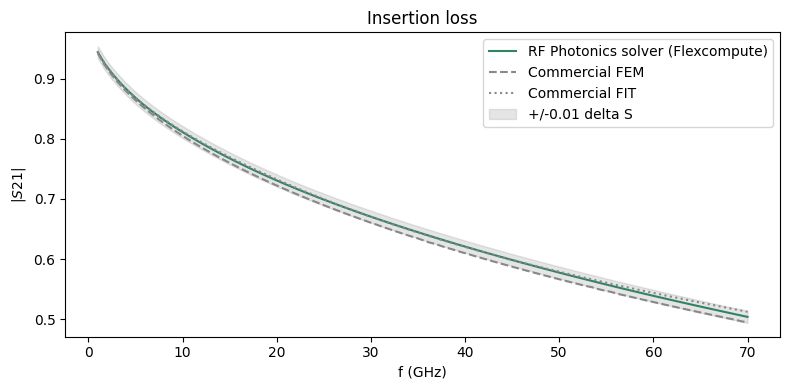
In controlled testing, the RF solver is able to solve this relatively large model in about 3.5 minutes on two A100 GPUs.
For comparison, this problem took about 1 hour to solve using the commercial FIT software, and close to 12 hours using the commercial FEM software. Benchmarking was done using a 20-core desktop workstation with 256 GB of RAM.
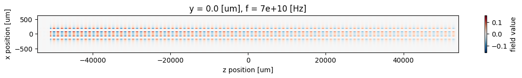
Below, we plot Ex in the signal plane at maximum frequency (f = 70 GHz).
# Load sim data for wave port 1
sim_data = tcm_3d_data.data["WP1@0"]
# Field plot
fig, ax = plt.subplots(figsize=(14, 1))
ex = sim_data["longitudinal field (y=0)"].Ex.sel(f=f_max, method="nearest")
np.real(ex).plot(
    x="z",
    y="x",
    ax=ax,
)
ax.set_ylim(-25 * mil, 25 * mil)
plt.show()