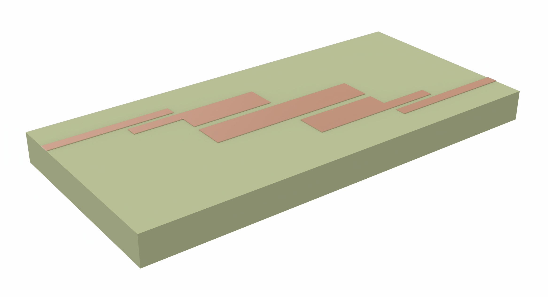
In this notebook, we demonstrate a hybrid microstrip/co-planar waveguide (CPW) bandpass filter designed to operate within the ultra-wideband (UWB) from 3.1-10.6 GHz. The UWB is permitted for unlicensed use in indoor and handheld devices by the Federal Communications Commission (FCC) since 2002. This filter design is proposed by Wang et al. in [1].
The filter uses a 5-pole design. It is driven by input and output microstrip transmission lines. The coupling region between the microstrip signal line, in the top layer, and the CPW, in the bottom layer, accounts for two of the five poles. The remaining three poles come from stepwise changes in the CPW gap width and line length.
import matplotlib.pyplot as plt
import numpy as np
import tidy3d as td
import tidy3d.rf as rf
import tidy3d.web as web

td.config.logging.level = "ERROR"
Building the Simulation
General Parameters
We define the frequency range of the simulation below, which covers the bandwidth of interest.
# Frequencies and bandwidth
(f_min, f_max) = (1e9, 13e9)
f0 = (f_min + f_max) / 2
freqs = np.linspace(f_min, f_max, 401)
Geometry parameters are defined below. The default length unit is microns, so we define the mm conversion factor for convenience.
mm = 1000 # Conversion factor from mm to micron
len_inf = 1e6 # Effective infinity
# Main dimensions
H = 0.635 * mm # Substrate thickness
T = 0.035 * mm # Metal thickness
W = 20 * mm # Overall width (y)
L = 30 * mm # Overall length (x)
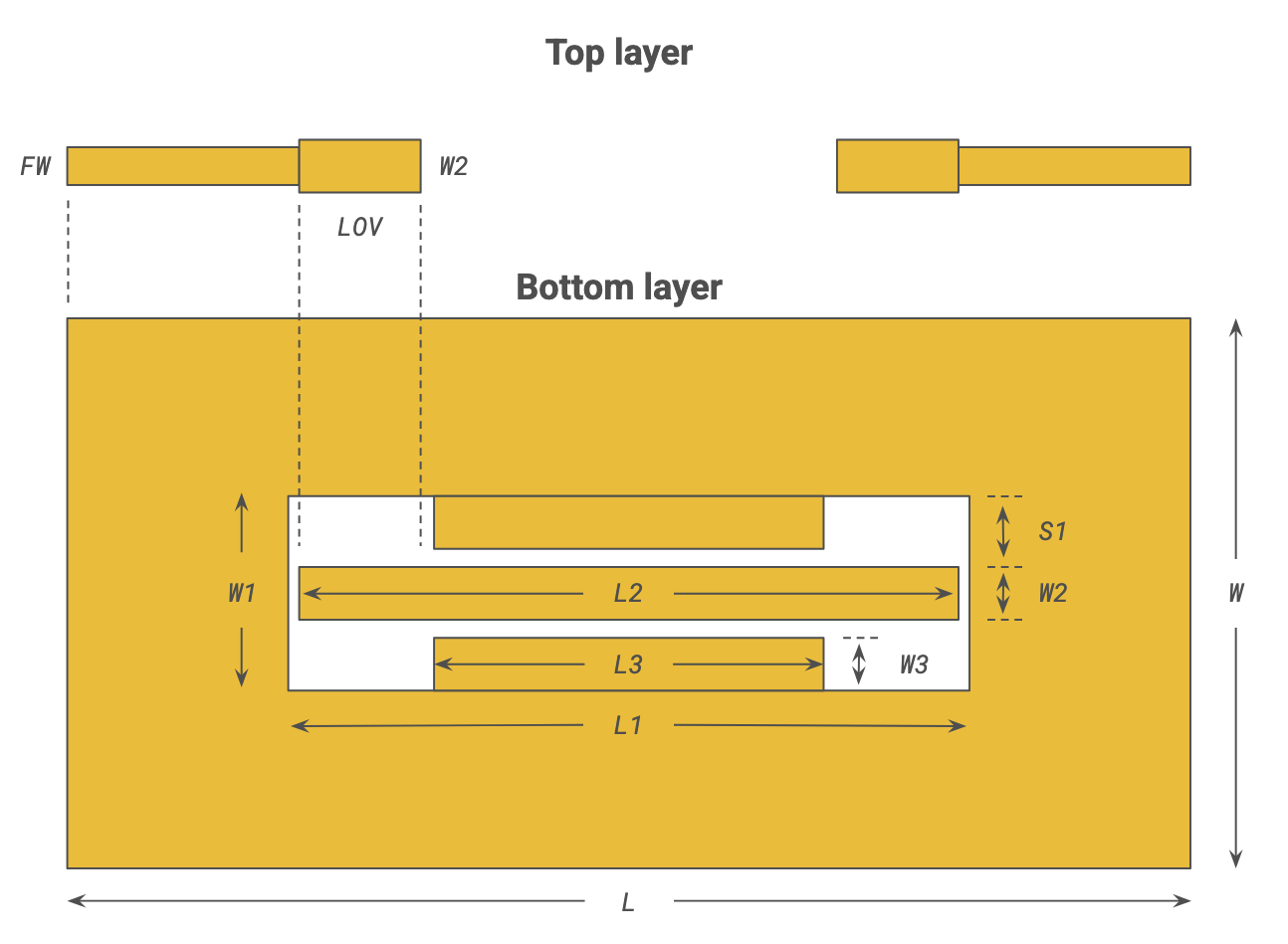
# Filter dimensions
S1 = 1.1 * mm # CPW wide gap
L1, W1 = (17.54 * mm, 0.92 * mm + 2 * S1) # CPW negative space
L2, W2 = (16.9 * mm, 0.92 * mm) # CPW middle strip
L3, W3 = (9.18 * mm, 0.92 * mm) # CPW top and bottom strips
# Feed dimensions (microstrip)
FW = 0.6 * mm # Feed width
LOV = 3.7 * mm # Overlap length
The simulation size is defined below.
# Sim size
sim_LX = 50 * mm
sim_LY = 40 * mm
sim_LZ = 20 * mm
Medium and Structures
The substrate is made of RT-Duroid 6010 and assumed lossless.
The metal (copper) is assumed to have constant conductivity of 60 S/um over the frequency range. The LossyMetalMedium implements a surface impedance boundary condition on the material and fields inside the material are assumed to be zero. This is most accurate when the metal thickness is larger than the skin depth.
med_air = td.Medium(permittivity=1, name="Air")
med_sub = td.Medium(permittivity=10.8, name="RT-Duroid 6010")
med_metal = rf.LossyMetalMedium(conductivity=60, frequency_range=(f_min, f_max), name="Lossy metal")
The structures for the simulation are defined below. First, the substrate.
# Substrate
str_sub = td.Structure(
    geometry=td.Box(center=(0, 0, 0), size=(L, W, H)),
    medium=med_sub,
)
The bottom metal layer is the CPW filter. We use geom_hole to cut out a rectangular hole in the ground plane geom_plane. This is done with the - operator, which is shorthand for a difference ClipOperation. Then we add three strips geom_top_box, geom_mid_box, and geom_bot_box to form the rest of the CPW in a single GeometryGroup.
# Bottom plane w/ CPW filter
z_bot = -H / 2 - T / 2
geom_plane = td.Box(center=(0, 0, z_bot), size=(L, W, T))
geom_hole = td.Box(center=(0, 0, z_bot), size=(L1, W1, T))
geom_top_box = td.Box(center=(0, W1 / 2 - W3 / 2, z_bot), size=(L3, W3, T))
geom_bot_box = geom_top_box.translated(0, -W1 + W3, 0)
geom_mid_box = td.Box(center=(0, 0, z_bot), size=(L2, W2, T))
geom_bottom_plane = td.GeometryGroup(
    geometries=[
        geom_top_box,
        geom_bot_box,
        geom_mid_box,
        geom_plane - geom_hole,
    ]
)
str_bottom_plane = td.Structure(geometry=geom_bottom_plane, medium=med_metal)
The top layer consists of the microstrip signal line. In the overlap section, the line is slightly widened to match the width of the CPW signal strip.
# Top plane w/ microstrips
z_top = H / 2 + T / 2
str_feed_1 = td.Structure(
    geometry=td.Box(center=((-L - L2) / 4, 0, z_top), size=((L - L2) / 2, FW, T)), medium=med_metal
)
str_feed_2 = td.Structure(
    geometry=td.Box(center=((L + L2) / 4, 0, z_top), size=((L - L2) / 2, FW, T)), medium=med_metal
)
str_overlap_patch_1 = td.Structure(
    geometry=td.Box(center=(-L2 / 2 + LOV / 2, 0, z_top), size=(LOV, W2, T)), medium=med_metal
)
str_overlap_patch_2 = td.Structure(
    geometry=td.Box(center=(L2 / 2 - LOV / 2, 0, z_top), size=(LOV, W2, T)), medium=med_metal
)
Finally, we collect all the structures in a list for later reference.
# Full structure list
str_list_full = [
    str_sub,
    str_bottom_plane,
    str_feed_1,
    str_feed_2,
    str_overlap_patch_1,
    str_overlap_patch_2,
]
Grid
For layered metallic structures such as this, the LayerRefinementSpec feature can be useful to quickly add refinement to metal corners and edges. The key settings here are min_steps_along_axis=2 and dl=T/2 for corner_refinement. This ensures a good level of refinement for accurate S-parameters.
Note that the settings chosen here favor accuracy over cost. For initial design exploration, we recommend reducing min_steps_along_axis to 1 and dl=T for much lower cost and slightly faster simulation time.
# Layer refinement for top and bottom metal layers
LR1_spec = rf.LayerRefinementSpec(
    center=(0, 0, z_top),
    size=(td.inf, td.inf, T),
    axis=2,
    corner_refinement=td.GridRefinement(dl=T / 2, num_cells=2),
    min_steps_along_axis=2,
)
LR2_spec = rf.LayerRefinementSpec(
    center=(0, 0, z_bot),
    size=(td.inf, td.inf, T),
    axis=2,
    corner_refinement=td.GridRefinement(dl=T / 2, num_cells=2),
    min_steps_along_axis=2,
)
The rest of the simulation uses an automatic grid, with maximum grid size set by the minimum wavelength.
grid_spec = td.GridSpec.auto(
    wavelength=td.C_0 / f_max, min_steps_per_wvl=20, layer_refinement_specs=[LR1_spec, LR2_spec]
)
Monitors
We define several field monitors for visualization purposes.
# Transverse field monitor
mon_1 = td.FieldMonitor(
    center=(6.7 * mm, 0, 0),
    size=(0, td.inf, td.inf),
    freqs=[f_min, f0, f_max],
    name="field transverse",
)

# Longitudinal field monitor
mon_2 = td.FieldMonitor(
    center=(0, 0, z_top),
    size=(td.inf, td.inf, 0),
    freqs=[f_min, f0, f_max],
    name="field microstrip plane",
)
mon_3 = td.FieldMonitor(
    center=(0, 0, z_bot), size=(td.inf, td.inf, 0), freqs=[f_min, f0, f_max], name="field CPW plane"
)
Ports
The model is excited by two 50 Ohm lumped ports, one for each microstrip line.
LP1 = rf.LumpedPort(
    center=(-L / 2, 0, 0),
    size=(0, FW, H),
    voltage_axis=2,
    name="LP1",
    impedance=50,
)
LP2 = LP1.updated_copy(center=(L / 2, 0, 0), name="LP2")
Simulation and TerminalComponentModeler
We collect all the previously defined information into a single Simulation object. A few notes:
- The model is surrounded by PML on all sides to absorb any radiated field.
- The model is symmetric about the y-axis, so we set up the
symmetryparameter accordingly. The value1refers to even symmetry (PMC). - The
shutoff(energy condition for early termination) is lowered to1e-7for better small signal accuracy.
sim = td.Simulation(
    size=(sim_LX, sim_LY, sim_LZ),
    grid_spec=grid_spec,
    boundary_spec=td.BoundarySpec.all_sides(boundary=td.PML()),
    structures=str_list_full,
    monitors=[mon_1, mon_2, mon_3],
    shutoff=1e-7,
    run_time=10e-9,
    symmetry=(0, 1, 0),
    plot_length_units="mm",
)
For RF simulations, we do not run the Simulation directly. Instead, we use the TerminalComponentModeler. This is a wrapper object that automatically sets up a port and frequency sweep to yield the full S-parameter matrix.
tcm = rf.TerminalComponentModeler(
    simulation=sim,
    ports=[LP1, LP2],
    freqs=freqs,
)
Visualization
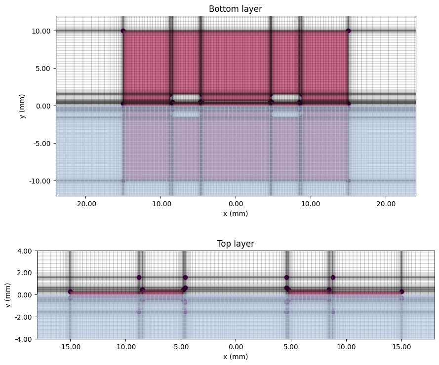
Before running, it is a good idea to plot the simulation to check the geometry and grid.
sim.plot_3d()
# Plot top and bottom planes
fig, ax = plt.subplots(2, 1, figsize=(9, 8), tight_layout=True)
sim.plot_grid(z=z_bot, ax=ax[0])
sim.plot(z=z_bot, ax=ax[0], monitor_alpha=0, hlim=(-0.8 * L, 0.8 * L), vlim=(-0.6 * W, 0.6 * W))
ax[0].set_title("Bottom layer")
sim.plot_grid(z=z_top, ax=ax[1])
sim.plot(z=z_top, ax=ax[1], monitor_alpha=0, hlim=(-0.6 * L, 0.6 * L), vlim=(-0.2 * W, 0.2 * W))
ax[1].set_title("Top layer")
plt.show()
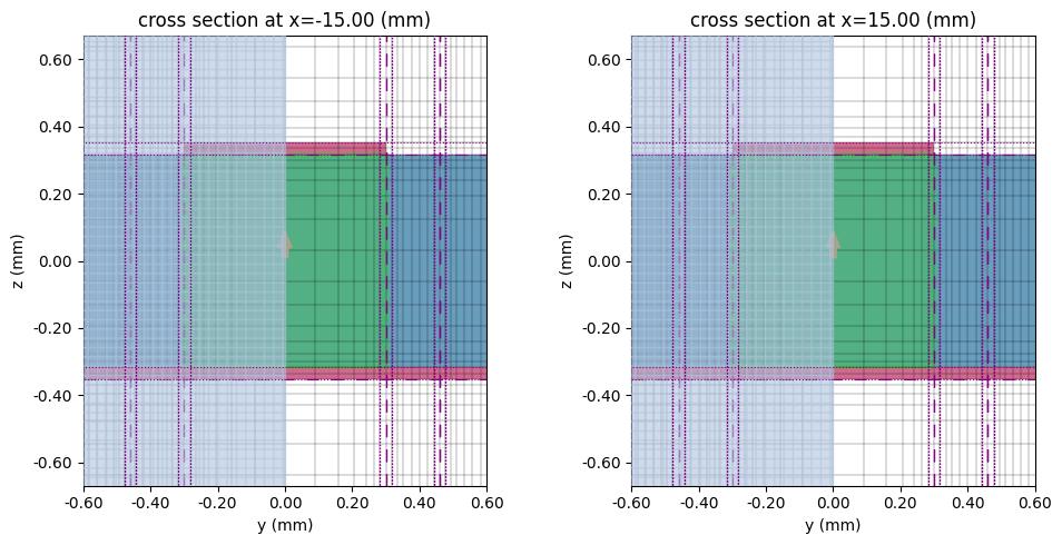
# Plot lumped ports
fig, ax = plt.subplots(1, 2, figsize=(10, 5), tight_layout=True)
tcm.plot_sim(x=-L / 2, ax=ax[0], monitor_alpha=0)
sim.plot_grid(x=-L / 2, ax=ax[0], hlim=(-FW, FW), vlim=(2 * z_bot, 2 * z_top))
tcm.plot_sim(x=L / 2, ax=ax[1], monitor_alpha=0)
sim.plot_grid(x=L / 2, ax=ax[1], hlim=(-FW, FW), vlim=(2 * z_bot, 2 * z_top))
plt.show()
Run Simulation
Use the tidy3d.web.upload() method to upload the job and get a cost estimate.
task_id = web.upload(tcm, task_name="hybrid_microstrip_filter", verbose=True)
17:33:20 EST Created task 'hybrid_microstrip_filter' with resource_id
             'sid-9399baa9-e38f-4f96-b7b5-b3966cf1744b' and task_type
             'TERMINAL_CM'.
             View task using web UI at
             'https://tidy3d.simulation.cloud/rf?taskId=pa-bc115415-7d48-4e80-95
             dd-56b2750590d9'.
Task folder: 'default'.
17:33:30 EST Maximum FlexCredit cost: 0.820. Minimum cost depends on task
             execution details. Use 'web.real_cost(task_id)' after run.
Next, we start the job and monitor its progress.
web.start(task_id)
web.monitor(task_id, verbose=True)
             Subtasks status - hybrid_microstrip_filter
             Group ID: 'pa-bc115415-7d48-4e80-95dd-56b2750590d9'
Batch status = preprocess
17:33:39 EST Batch status = running
17:36:14 EST Batch status = postprocess
17:36:31 EST Modeler has finished running successfully.
Billed flex credit cost: 0.656.
After the simulation is complete, we load the data and compute the S-matrix.
# Load TCM data
tcm_data = web.load(task_id)
# Calculate S-matrix
s_matrix = tcm_data.smatrix()
17:36:34 EST Loading component modeler data from cm_data.hdf5
Results
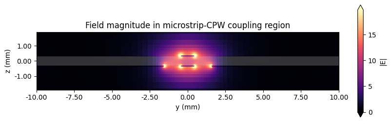
Field Profiles
First, let us examine the field profiles. The field monitor data for a given port excitation can be accessed from the corresponding SimulationData instance. The latter is obtained using the appropriate key (the port name) on the data attribute of the TCM data instance.
sim_data = tcm_data.data["LP1"]
The field profiles are plotted below.
# Transverse field
fig, ax = plt.subplots(figsize=(10, 3))
sim_data.plot_field("field transverse", field_name="E", val="abs", scale="lin", f=f0, ax=ax)
ax.set_xlim(-W / 2, W / 2)
ax.set_ylim(-3 * H, 3 * H)
ax.set_title("Field magnitude in microstrip-CPW coupling region")
plt.show()
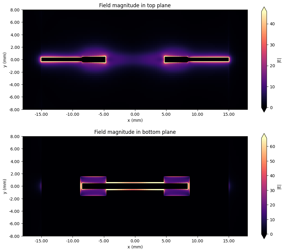
# In-plane fields
fig, ax = plt.subplots(2, 1, figsize=(12, 10))
sim_data.plot_field("field microstrip plane", field_name="E", val="abs", f=f0, ax=ax[0])
sim_data.plot_field("field CPW plane", field_name="E", val="abs", f=f0, ax=ax[1])
for axis in ax:
    axis.set_xlim(-0.6 * L, 0.6 * L)
    axis.set_ylim(-0.4 * W, 0.4 * W)
ax[0].set_title("Field magnitude in top plane")
ax[1].set_title("Field magnitude in bottom plane")
plt.show()
S-parameters and Group Delay
The desired S-parameter $S_{ij}$ can be extracted from the full s_matrix using the port_in and port_out indices. Since the default phase convention in the solver is the physics convention $e^{-i\omega t}$, we apply np.conjugate to convert the S-parameters to the engineering convention $e^{j\omega t}$.
S11 = np.conjugate(s_matrix.data.isel(port_in=0, port_out=0))
S21 = np.conjugate(s_matrix.data.isel(port_in=0, port_out=1))
S11dB = 20 * np.log10(np.abs(S11))
S21dB = 20 * np.log10(np.abs(S21))
For benchmarking purposes, we import comparison data from an identical model run using a commercial FEM solver.
f_fem, S11dB_fem, S21dB_fem = np.genfromtxt(
    fname="./misc/mccpw_fem.csv", delimiter=",", unpack=True
)
The insertion and return losses are plotted below. We observe a good match with the commercial FEM benchmark.
fig, ax = plt.subplots(figsize=(10, 5), tight_layout=True)
ax.plot(freqs / 1e9, S21dB, "b", label="|S21|$^2$")
ax.plot(f_fem, S21dB_fem, "b--", label="|S21|$^2$ (Commercial FEM)")
ax.plot(freqs / 1e9, S11dB, "r", label="|S11|$^2$")
ax.plot(f_fem, S11dB_fem, "r--", label="|S11|$^2$ (Commercial FEM)")
ax.add_patch(plt.Rectangle((3.1, 0), 10.6 - 3.1, -50, fc="gray", alpha=0.2, label="UWB bandwidth"))
ax.legend()
ax.set_xlabel("f (GHz)")
ax.set_ylabel("dB")
plt.show()
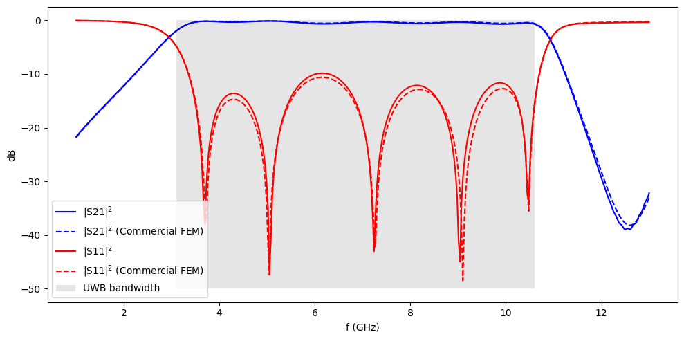
The filter exhibits a passband that is almost flat and a maximum S11 of approximately -10dB throughout the UWB passband. This is also in good agreement with the experimental results reported in the reference paper.
We can also calculate the group delay $$ \tau_g(\omega) \simeq -\frac{\Delta\phi}{\Delta\omega} $$ where $\phi$ is the phase of S21 and $\omega = 2\pi f$.
# Calculating group delay
df = freqs[1] - freqs[0]
group_delay_S21 = -np.diff(np.unwrap(np.angle(S21))) / (2 * np.pi * df) * 1e9

fig, ax = plt.subplots(figsize=(10, 5), tight_layout=True)
ax.plot(freqs[:-1] / 1e9, group_delay_S21, label="Group delay")
ax.add_patch(
    plt.Rectangle((3.1, 0.1), 10.6 - 3.1, 0.6, fc="gray", alpha=0.2, label="UWB bandwidth")
)
ax.legend()
ax.set_xlabel("f (GHz)")
ax.set_ylabel("ns")
plt.show()
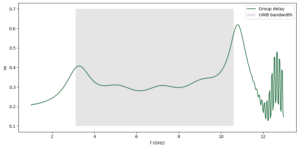
We observe that the group delay varies between 0.3 to 0.6 ns in the UWB passband. This is close to the 0.46 to 0.74 ns range reported in experimental measurements in the paper. In either case, the maximum variation in group delay is less than 0.3 ns.
Outside the UWB passband, we can observe oscillatory behaviour near the limits of the simulation bandwidth. This is due to the small value of |S21|. We can reduce this oscillation by further lowering the shutoff value in Simulation and extending run_time. That said, for this demonstration, it is not a priority since we are primarily interested in behavior within the UWB passband.
Reference
[1] Hang Wang, Lei Zhu and W. Menzel, "Ultra-wideband bandpass filter with hybrid microstrip/CPW structure," in IEEE Microwave and Wireless Components Letters, vol. 15, no. 12, pp. 844-846, Dec. 2005, doi: 10.1109/LMWC.2005.860016.