Research Highlight: Scale-invariant Dielectric Waveguide
The field of integrated photonic circuits has seen a significant and rapid expansion in recent years, with strong indications of continued acceleration in the near future. This growth is largely fueled by innovative academic research.
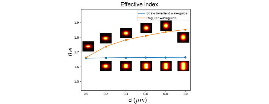
A notable example of such advancement is the study led by Dr. Janderson Rodrigues and Dr. Utsav Dave from Professor Michal Lipson’s team at Columbia University, as detailed in a recent publication in Nature Communications. This research introduces a new dielectric waveguiding mechanism. Their novel waveguide design effectively traps light within materials of low refractive index on a chip. The study reveals that at a specific threshold, the transverse wavevector transitions from imaginary to real, consequently forming an optical mode that remains consistent and scale-independent, regardless of the geometry. This phenomenon results in significant light localization within a low-index layer, presenting a substantial advancement in the field.

The waveguide design presented in the study is highly intriguing. We replicated the simulations described in the original paper, presenting them as a public example. Our simulation results align closely with both the theoretical predictions and the experimental observations reported in the study.
We had the privilege of interviewing Dr. Janderson Rodrigues and Dr. Utsav Dave, who graciously offered insights into their research. We are immensely grateful for the time and effort they devoted to this discussion. The following is the complete interview transcript, encompassing the questions and their insightful responses.
1. What inspired the initial concept for the scale-invariant waveguide design in the paper?
We were working on an unrelated project in which the goal was to reduce the evanescent fields in order to avoid the coupling between parallel waveguides. By analyzing the corresponding equations, it turns out that it is easier to increase the evanescent field instead of decreasing it. At the limit, the field becomes flat before it becomes radiation modes. This inflection point is exactly the cut-off condition of the asymmetric waveguide and therefore is an unstable point (the critical angle). We realized that two parallel waveguides operating at this condition would lead to a flat mode. Later we found out that something similar has been predicted in plasmonic waveguides, which helped us to understand the effect with the huge advantage of using only (lossless) dielectric materials.
2. What advantage does the scale-invariant waveguide have over conventional dielectric waveguide?
Janderson: One of the main advantages of the scale-invariant waveguide is the increasing overlap of the field intensity with low-index materials, mainly in heterogeneous structures, due to the limited number of alternative approaches. For this purpose, beyond the critical point is even more attractive. Furthermore, a flat mode distribution means a uniform distribution of light throughout the middle material (large mode effective area), which can be interesting to avoid non-linear effects or tailor the saturation of gain medium, for instance. Besides that, the starting point of increasing the evanescent coupling (i.e., shorter directional couplers) still can be explored.
Utsav: Besides, since the scale invariant waveguide has the same effective index as the low-index material width is changed, devices with different dimensions can retain the same overall phase shift, which can be useful in optimizing different structures without worrying about realigning phase shifts.
3. How do the uniform field distribution and non-Gaussian spatial profile in your waveguides impact their potential applications in integrated photonics? How do you envision the application of scale-invariant waveguides in the future?
Although, the paper shows the experimental demonstration in the telecommunication range, the same concept can be applied to other regions of the electromagnetic spectrum, for example, the visible or the terahertz range. We also notice that the proposed structure might find applications in electro-optic modulation, nonlinear integrated photonics, and temperature control.
4. What are you working on currently?
Janderson: Currently, I am working in the private sector in the field of integrated photonics and trying to find a good balance between my interest in basic science with the necessity of product development and engineering.
Utsav: I am working in a proteomics company where we use integrated photonics for single-molecule sensing of proteins, helping to usher in the next revolution beyond genomics.
5. Can you give some suggestions to students who want to work in the field of photonics?
Janderson: If I can give any suggestions for students in the field, it would be to use toy models. The fact that we can play with these relatively simple equations of 1D slab waveguides before going to more rigorous numerical simulations, was one of the greatest pieces of advice that was given to me.
Utsav: Photonics is both a great applications-oriented platform as well as a playground for exploring all kinds of cool physics like nonlinear dynamics, non-Hermitian or topological physics, etc. So you may not know from the beginning what kind of work/topic you like and the best way to know is to try a bunch of things. Try and get a broad overview of all aspects - from theory to fabrication and experiment. This will help you whether you end up in industry or academia (or something else). It’s also important to make sure that the research group culture where you will be spending your master’s or PhD matches your personality and is nurturing - that by far is the most important factor to success.
Author Bios
 Janderson Rocha Rodrigues was born in Sao Paulo, Brazil, in 1980. He received the Microelectronics Engineering Diploma from the Sao Paulo State Technological College (FATECSP), Sao Paulo, Brazil, in 2008 and the M.S. and Ph.D. degrees in Space Science & Technologies Engineering from the Aeronautics Institute of Technology (ITA), Sao Jose dos Campos, SP, Brazil in 2011 and 2019. From 2018 to 2019, he was a Ph.D. visiting student at Michal Lipson’s group at Columbia University, NY, USA, where he rejoined as a postdoctoral Research Scientist from 2019 to 2023. Since 2023, he has been a Research Scientist at Corning Inc., NY, USA. His research interests include applications of integrated photonics to communications as well as to sensing and instrumentation.

Utsav D. Dave, originally from western India, completed his B. Tech. nestled in the foothills of the Himalayas in 2010 from the Indian Institute of Technology, Guwahati. He then went on to do a M.S. in Photonics jointly from a group of UK and European universities through the Erasmus Mundus program followed by a PhD in integrated silicon photonics from Ghent University, Belgium. He later moved to Michal Lipson’s group at Columbia University as a postdoc in 2017 where he worked on subwavelength and non-Hermitian photonics, LiDAR and frequency combs before joining Quantum-Si in 2022 where he currently works on photonics for proteomics using single-molecular spectroscopy.

Prof. Michal Lipson is the Eugene Higgins Professor at Columbia University. Her research focus is on Nanophotonics and includes the investigation of novel phenomena, as well as the development of novel devices and applications. She is the inventor of over 45 issued patents and has co-authored more than 250 scientific publications. In recognition of her work in silicon photonics, she was elected as a member of the National Academy of Sciences and the American Academy of Arts and Sciences. Her numerous awards include the NAS Comstock Prize in Physics, the MacArthur Fellowship, the Blavatnik Award, Optica’s R. W. Wood Prize, the John Tyndall Award, the IEEE Photonics Award, and an honorary degree from Trinity College, University of Dublin. In 2020 she was elected the 2021 Vice President of Optica, formerly known as The Optical Society, and will serve as Optica President in 2023. Since 2014, every year she has been named by Thomson Reuters as a top 1% highly cited researcher in the field of Physics.