TIDY3D
LEARNING CENTER


Inverse Design in Photonics Lecture 5: Shape Optimization
By Tyler Hughes, Zongfu Yu and Shanhui FanIn this lecture, we introduce a method to optimize your device with respect to a geometric parameterization using inverse design and the adjoint method. As an example, we demonstrate the inverse design of a 90 degree waveguide bend by shifting the boundaries of the device.
Adjoint-based Shape Optimization of a Waveguide Bend
In this notebook, we will apply the adjoint method to the optimization of a low-loss waveguide bend. We start with a 90 degree bend in a SiN waveguide, parameterized using a td.PolySlab.
We define an objective function that seeks to maximize the transmission of the TE0 output mode amplitude with respect to the position of the polygon vertices defining the bend. A penalty is applied to keep the local radii of curvature larger than a pre-defined value.
The resulting device demonstrates low loss and exhibits a smooth geometry.
To install the
jaxmodule required for this feature, we recommend runningpip install "tidy3d[jax]".
If you are unfamiliar with inverse design, we also recommend our intro to inverse design tutorials and our primer on automatic differentiation with tidy3d.
Setup
First, we import tidy3d and it's adjoint plugin. We will also use numpy, matplotlib and jax.
import tidy3d as td
import tidy3d.plugins.adjoint as tda
from tidy3d.plugins.adjoint.web import run_local as run
import numpy as np
import matplotlib.pylab as plt
import jax
import jax.numpy as jnp
Next, we define all the global parameters for our device and optimization.
wavelength = 1.5
freq0 = td.C_0 / wavelength

# frequency of measurement and source
# note: we only optimize results at the central frequency for now.
fwidth = freq0 / 10
num_freqs = 10
freqs = np.linspace(freq0 - fwidth/2, freq0 + fwidth/2, num_freqs)

# define the discretization of the bend polygon in angle
num_pts = 60
angles = np.linspace(0, np.pi/2, num_pts + 2)[1:-1]

# refractive indices of waveguide and substrate (air above)
n_wg = 2.0
n_sub = 1.5

# min space between waveguide and PML
spc = 1 * wavelength

# length of input and output straight waveguide sections
t = 1 * wavelength

# distance between PML and the mode source / mode monitor
mode_spc = t / 2.0

# height of waveguide core
h = 0.7

# minimum, starting, and maximum allowed thicknesses for the bend geometry
wmin = 0.5
wmid = 1.5
wmax = 2.5

# average radius of curvature of the bend
radius = 6

# minimum allowed radius of curvature of the polygon
min_radius = 150e-3

# name of the monitor measuring the transmission amplitudes for optimization
monitor_name = "mode"

# how many grid points per wavelength in the waveguide core material
min_steps_per_wvl = 30

# how many mode outputs to measure
num_modes = 3
mode_spec = td.ModeSpec(num_modes=num_modes)
Using all of these parameters, we can define the total simulation size.
Lx = Ly = t + radius + abs(wmax - wmid) + spc
Lz = spc + h + spc
Define parameterization
Next we describe how the geometry looks as a function of our design parameters.
At each angle on our bend discretization, we define a parameter that can range between -inf and +inf to control the thickness of that section. If that parameter is -inf, 0, and +inf, the thickness of that section is wmin, wmid, and wmax, respectively.
This gives us a smooth way to constrain our measurable parameter without needing to worry about it in the optimization.
def thickness(param: float) -> float:
    """thickness of a bend section as a function of a parameter in (-inf, +inf)."""
    param_01 = (jnp.tanh(param) + 1.0) / 2.0
    return wmax * param_01 + wmin * (1 - param_01)
Next we write a function to generate all of our bend polygon vertices given our array of design parameters. Note that we add extra vertices at the beginning and end of the bend that are independent of the parameters (static) and are only there to make it easier to connect the bend to the input and output waveguide sections.
def make_vertices(params: np.ndarray) -> list:
    """Make bend polygon vertices as a function of design parameters."""
    vertices = []
    vertices.append((-Lx/2 + 1e-2, -Ly/2 + t + radius))
    vertices.append((-Lx/2 + t, -Ly/2 + t + radius + wmid/2))
    for angle, param in zip(angles, params):
        thickness_i = thickness(param)
        radius_i = radius + thickness_i/2.0
        x = radius_i * np.sin(angle) -Lx/2 + t
        y = radius_i * np.cos(angle) -Ly/2 + t
        vertices.append((x, y))
    vertices.append((-Lx/2 + t + radius + wmid/2, -Ly/2 + t))
    vertices.append((-Lx/2 + t + radius, -Ly/2 + 1e-2))
    vertices.append((-Lx/2 + t + radius - wmid/2, -Ly/2 + t))
    for angle, param in zip(angles[::-1], params[::-1]):
        thickness_i = thickness(param)
        radius_i = radius - thickness_i/2.0
        x = radius_i * np.sin(angle) -Lx/2 + t
        y = radius_i * np.cos(angle) -Ly/2 + t
        vertices.append((x, y))
    vertices.append((-Lx/2 + t, -Ly/2 + t + radius - wmid/2))
    return vertices
Let's try out our make_vertices function on a set of all 0 parameters, which should give the starting waveguide width of wmid across the bend.
params = np.zeros(num_pts)
vertices = make_vertices(params)
No GPU/TPU found, falling back to CPU. (Set TF_CPP_MIN_LOG_LEVEL=0 and rerun for more info.)
plt.scatter(*np.array(vertices).T)
ax = plt.gca()
ax.set_aspect("equal")
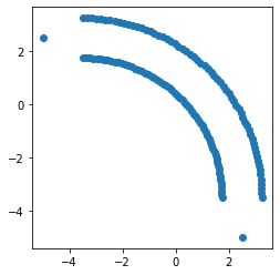
Looks good, note again that the extra points on the ends are just to ensure a solid overlap with the in and out waveguides. At this time, the adjoint plugin does not handle polygons that extend outside of the simulation domain so we need to also ensure that all points are inside of the domain.
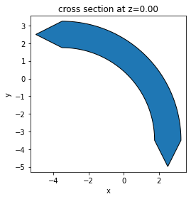
Next we wrap this to write a function to generate a 3D JaxPolySlab geometry given our design parameters. The JaxPolySlab is simply a jax-compatible version of the regular PolySlab geometry that can be differentiated through.
def make_polyslab(params: np.ndarray) -> tda.JaxPolySlab:
    """Make a `tidy3d.PolySlab` for the bend given the design parameters."""
    vertices = make_vertices(params)
    return tda.JaxPolySlab(
        vertices=vertices,
        slab_bounds=(-h/2, h/2),
        axis=2,
    )
Let's visualize this as well.
polyslab = make_polyslab(params)
ax = polyslab.plot(z=0)

Keeping with this theme, we add a function to generate a list of JaxStructures with just one element (our differentiable polygon bend).
def make_input_structures(params) -> list[tda.JaxStructure]:
    polyslab = make_polyslab(params)
    medium = tda.JaxMedium(permittivity=n_wg**2)
    return [tda.JaxStructure(geometry=polyslab, medium=medium)]
(ring,) = input_structures = make_input_structures(params)
ax = ring.plot(z=0)
Next, we define the other "static" geometries, such as the input waveguide section, output waveguide section, and substrate.
box_in = td.Box.from_bounds(
    rmin=(-Lx/2 - 1, -Ly/2 + t + radius - wmid/2, -h/2),
    rmax=(-Lx/2 + t + 1e-3, -Ly/2 + t + radius + wmid/2, +h/2),
)
box_out = td.Box.from_bounds(
    rmin=(-Lx/2 + t + radius - wmid/2, -Ly/2 - 1, -h/2),
    rmax=(-Lx/2 + t + radius + wmid/2, -Ly/2 + t, +h/2),
)

geo_sub = td.Box.from_bounds(
    rmin=(-td.inf, -td.inf, -10000),
    rmax=(+td.inf, +td.inf, -h/2),
)

wg_in = td.Structure(geometry=box_in, medium=td.Medium(permittivity=n_wg**2))
wg_out = td.Structure(geometry=box_out, medium=td.Medium(permittivity=n_wg**2))
substrate = td.Structure(geometry=geo_sub, medium=td.Medium(permittivity=n_sub**2))
Fabrication Constraints
With the current parameterization, it is possible to generate structures with wildly varying radii of curvature which may be difficult to fabricate. To alleviate this, we introduce a minimum radius of curvature penalty transformation using the tidy3d adjoint utilities. The penalty will take a set of vertices, compute the local radius of curvature using a quadratic Bezier curve, and return an average penalty function that depends on how much smaller the local radii are compared to a desired minimum radius.
from tidy3d.plugins.adjoint.utils.penalty import RadiusPenalty

penalty = RadiusPenalty(min_radius=min_radius, alpha=1.0, kappa=10.0)
We then wrap this penalty to look at only the inner and outer vertices independently and average the penalty from each.
def eval_penalty(params):
    """Evaluate penalty on a set of params looking at radius of curvature."""
    vertices = make_vertices(params)
    _vertices =  jnp.array(vertices)
    vertices_top = _vertices[1:num_pts+3] # select outer set of points along bend
    vertices_bot = _vertices[num_pts+4:]  # select inner set of points along bend
    penalty_top = penalty.evaluate(vertices_top)
    penalty_bot = penalty.evaluate(vertices_bot)
    return (penalty_top + penalty_bot) / 2.0
Let's try this out on our starting parameters. We see we get a jax traced float that seems reasonably low given our smooth starting structure.
eval_penalty(params)
Array(3.5788543e-23, dtype=float32)
Define Simulation
Now we define our sources, monitors, and simulation.
We first define a mode source injected at the input waveguide.
mode_width = wmid + 2 * spc
mode_height = Lz

mode_src = td.ModeSource(
    size=(0, mode_width, mode_height),
    center=(-Lx/2 + t/2, -Ly/2 + t + radius, 0),
    direction="+",
    source_time=td.GaussianPulse(
        freq0=freq0,
        fwidth=fwidth,
    )
)
Next, we define monitors for storing:
-
The output mode amplitude at the central frequency.
-
The flux on the output plane (for reference).
-
The output mode amplitude across a frequency range (for examining the transmission spectrum of our final device).
-
A field monitor to measure fields directly in the z-normal plane intersecting the waveguide.
mode_mnt = td.ModeMonitor(
    size=(mode_width, 0, mode_height),
    center=(-Lx/2 + t + radius, -Ly/2 + t/2, 0),
    name=monitor_name,
    freqs=[freq0],
    mode_spec=mode_spec,
)

flux_mnt = td.FluxMonitor(
    size=(mode_width, 0, mode_height),
    center=(-Lx/2 + t + radius, -Ly/2 + t/2, 0),
    name="flux",
    freqs=[freq0],
)

mode_mnt_bb = td.ModeMonitor(
    size=(mode_width, 0, mode_height),
    center=(-Lx/2 + t + radius, -Ly/2 + t/2, 0),
    name="mode_bb",
    freqs=freqs.tolist(),
    mode_spec=mode_spec,
)

fld_mnt = td.FieldMonitor(
    size=(td.inf, td.inf, 0),
    freqs=[freq0],
    name="field",
)
[22:01:59] WARNING: Default value for the field monitor           monitor.py:261
           'colocate' setting has changed to 'True' in Tidy3D
           2.4.0. All field components will be colocated to the
           grid boundaries. Set to 'False' to get the raw fields
           on the Yee grid instead.
Next we put everything together into a function that returns a JaxSimulation given our parameters and an optional boolean specifying whether to include the field monitor (to save data when fields are not required).
def make_sim(params, use_fld_mnt: bool = True) -> tda.JaxSimulation:
    monitors = [mode_mnt_bb, flux_mnt]
    if use_fld_mnt:
        monitors += [fld_mnt]
    input_structures = make_input_structures(params)
    return tda.JaxSimulation(
        size=(Lx, Ly, Lz),
        input_structures=input_structures,
        structures=[substrate, wg_in, wg_out],
        sources=[mode_src],
        output_monitors=[mode_mnt],
        grid_spec=td.GridSpec.auto(min_steps_per_wvl=min_steps_per_wvl),
        boundary_spec=td.BoundarySpec.pml(x=True, y=True, z=True),
        monitors=monitors,
        run_time = 10/fwidth,
)
Let's try it out and plot our simulation.
sim = make_sim(params)

f, (ax1, ax2) = plt.subplots(1,2,tight_layout=True, figsize=(10,4))
ax = sim.plot(z=0.01, ax=ax1)
ax = sim.plot(x=-Lx/2+t/2, ax=ax2)
           WARNING: 'JaxPolySlab'-containing                   simulation.py:202
           'JaxSimulation.input_structures[0]' intersects with
           'JaxSimulation.structures[1]'. Note that in this
           version of the adjoint plugin, there may be errors
           in the gradient when 'JaxPolySlab' intersects with
           background structures.
           WARNING: Structure at structures[3] was detected as simulation.py:486
           being less than half of a central wavelength from a
           PML on side x-min. To avoid inaccurate results,
           please increase gap between any structures and PML
           or fully extend structure through the pml.
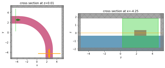
Note: we get warnings from the adjoint plugin because the polyslab intersects the static waveguide ports and those edges will give inaccurate gradients. We can safely ignore those warnings because we don't need gradients with respect to them.
td.config.logging_level = "ERROR"
Select the desired waveguide mode
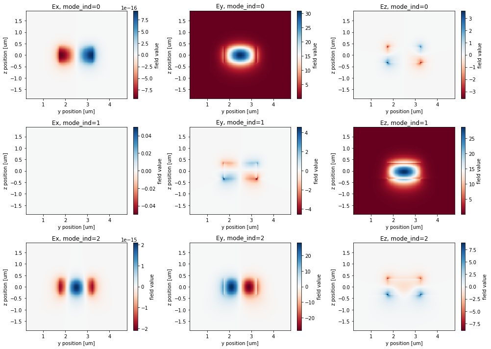
Next, we use the ModeSolver to solve and select the mode_index that gives us the proper injected and measured modes. We plot all of the fields for the first 3 modes and see that the TE0 mode is mode_index=0.
from tidy3d.plugins.mode import ModeSolver

ms = ModeSolver(simulation=sim, plane=mode_src, mode_spec=mode_spec, freqs=mode_mnt.freqs)
data = ms.solve()

print("Effective index of computed modes: ", np.array(data.n_eff))

fig, axs = plt.subplots(num_modes, 3, figsize=(14, 10), tight_layout=True)
for mode_ind in range(num_modes):
    for field_ind, field_name in enumerate(("Ex", "Ey", "Ez")):
        field = data.field_components[field_name].sel(mode_index=mode_ind)
        ax = axs[mode_ind, field_ind]
        field.real.plot(x='y', y='z', ax=ax, cmap='RdBu')
        ax.set_title(f"{field_name}, mode_ind={mode_ind}")
Effective index of computed modes: [[1.7966835 1.7514163 1.6002883]]
Since this is already the default mode index, we can leave the original make_sim() function as is. However, to generate a new mode source with a different mode_index, we could do the following and rewrite that function with the returned mode_src.
# select the mode index
mode_index = 0

# make the mode source with appropriate mode index
mode_src = ms.to_source(mode_index=mode_index, source_time=mode_src.source_time, direction=mode_src.direction)
Defining objective function
Now we can define our objective function to maximize. The objective function first generates a simulation given the parameters, runs the simulation using the jax-compatible tidy3d.plugins.adjoint.run function, measures the power transmitted into the TE0 output mode at our desired polarization, and then subtracts the radius of curvature penalty that we defined earlier.
For convenience, we also return the JaxSimulationData as the 2nd output, which will be ignored by jax when we pass has_aux=True when computing the gradient of this function.
def objective(params, use_fld_mnt:bool = True):
    sim = make_sim(params, use_fld_mnt=use_fld_mnt)
    sim_data = run(sim, task_name='bend', verbose=False)
    amps = sim_data[monitor_name].amps.sel(direction="-", mode_index=mode_index).values
    transmission = jnp.abs(jnp.array(amps))**2
    J = jnp.sum(transmission) - eval_penalty(params)
    return J, sim_data
Next, we use jax.value_and_grad to transform this objective function into a function that returns the
-
Objective function evaluated at the passed parameters.
-
Auxilary JaxSimulationData corresponding to the forward pass (for plotting later).
-
Gradient of the objective function with respect to the passed parameters.
val_grad = jax.value_and_grad(objective, has_aux=True)
Let's run this function and take a look at the outputs.
(val, sim_data), grad = val_grad(params)
print(val)
print(grad)
0.5606048
[-0.01883917 -0.02968327 -0.04119704 -0.05332555 -0.0657288  -0.07819955
 -0.09031129 -0.10045863 -0.11044198 -0.11628526 -0.11940013 -0.11855873
 -0.11367789 -0.10428579 -0.09043597 -0.07393086 -0.05485675 -0.03374749
 -0.01146651  0.01097884  0.03232303  0.0521329   0.07017162  0.08563211
  0.09907499  0.10945182  0.11626573  0.12678576  0.11849307  0.12726338
  0.12726587  0.11850015  0.12679777  0.11628053  0.10946865  0.0990923
  0.08564843  0.07018599  0.05214434  0.03233124  0.01098366 -0.01146469
 -0.03374784 -0.0548588  -0.07393336 -0.09043836 -0.10428729 -0.11367796
 -0.11855777 -0.11939806 -0.11628282 -0.11043957 -0.10045616 -0.09030911
 -0.07819756 -0.06572723 -0.05332468 -0.04119653 -0.02968323 -0.01883924]
These seem reasonable and can now be used for plugging into our optimization algorithm.
Optimization Procedure
With our gradients defined, we write a simple optimization loop using the optax package. We use the adam method with a tunable number of steps and learning rate. The intermediate values, parameters, and data are stored for visualization later.
Note: this will take several minutes. While not shown here, it is good practice to checkpoint your optimization results by saving to file on every iteration, or ensure you have a stable internet connection. See this notebook for more details.
import optax

# hyperparameters
num_steps = 40
learning_rate = 0.1

# initialize adam optimizer with starting parameters
params = np.array(params).copy()
optimizer = optax.adam(learning_rate=learning_rate)
opt_state = optimizer.init(params)

# store history
objective_history = []
param_history = [params]
data_history = []

for i in range(num_steps):

    # compute gradient and current objective funciton value
    (value, sim_data), gradient = val_grad(params)

    # multiply all by -1 to maximize obj_fn
    gradient = -np.array(gradient.copy())

    # outputs
    print(f"step = {i + 1}")
    print(f"\tJ = {value:.4e}")
    print(f"\tgrad_norm = {np.linalg.norm(gradient):.4e}")

    # compute and apply updates to the optimizer based on gradient
    updates, opt_state = optimizer.update(gradient, opt_state, params)
    params = optax.apply_updates(params, updates)

    # save history
    objective_history.append(value)
    param_history.append(params)
    data_history.append(sim_data)
step = 1
	J = 5.6060e-01
	grad_norm = 6.7526e-01
step = 2
	J = 8.4790e-01
	grad_norm = 4.8040e-01
step = 3
	J = 8.9985e-01
	grad_norm = 4.0505e-01
step = 4
	J = 8.5131e-01
	grad_norm = 5.0348e-01
step = 5
	J = 8.3506e-01
	grad_norm = 4.8749e-01
step = 6
	J = 8.6678e-01
	grad_norm = 4.8803e-01
step = 7
	J = 9.2224e-01
	grad_norm = 3.5351e-01
step = 8
	J = 9.5242e-01
	grad_norm = 1.8946e-01
step = 9
	J = 9.4218e-01
	grad_norm = 2.4269e-01
step = 10
	J = 9.1947e-01
	grad_norm = 2.9453e-01
step = 11
	J = 9.0531e-01
	grad_norm = 3.2005e-01
step = 12
	J = 9.1071e-01
	grad_norm = 3.1154e-01
step = 13
	J = 9.3085e-01
	grad_norm = 2.5689e-01
step = 14
	J = 9.5300e-01
	grad_norm = 1.7606e-01
step = 15
	J = 9.6490e-01
	grad_norm = 1.0440e-01
step = 16
	J = 9.6218e-01
	grad_norm = 1.3483e-01
step = 17
	J = 9.5238e-01
	grad_norm = 1.9516e-01
step = 18
	J = 9.4548e-01
	grad_norm = 2.2601e-01
step = 19
	J = 9.4680e-01
	grad_norm = 2.1709e-01
step = 20
	J = 9.5441e-01
	grad_norm = 1.7686e-01
step = 21
	J = 9.6259e-01
	grad_norm = 1.2697e-01
step = 22
	J = 9.6678e-01
	grad_norm = 9.8830e-02
step = 23
	J = 9.6526e-01
	grad_norm = 1.2304e-01
step = 24
	J = 9.6185e-01
	grad_norm = 1.4719e-01
step = 25
	J = 9.5993e-01
	grad_norm = 1.5421e-01
step = 26
	J = 9.6063e-01
	grad_norm = 1.4313e-01
step = 27
	J = 9.6385e-01
	grad_norm = 1.2455e-01
step = 28
	J = 9.6807e-01
	grad_norm = 1.0047e-01
step = 29
	J = 9.7131e-01
	grad_norm = 7.4751e-02
step = 30
	J = 9.7191e-01
	grad_norm = 6.6567e-02
step = 31
	J = 9.7001e-01
	grad_norm = 8.9463e-02
step = 32
	J = 9.6791e-01
	grad_norm = 1.0970e-01
step = 33
	J = 9.6786e-01
	grad_norm = 1.1280e-01
step = 34
	J = 9.7046e-01
	grad_norm = 9.2556e-02
step = 35
	J = 9.7376e-01
	grad_norm = 5.5497e-02
step = 36
	J = 9.7541e-01
	grad_norm = 2.5039e-02
step = 37
	J = 9.7487e-01
	grad_norm = 4.3832e-02
step = 38
	J = 9.7340e-01
	grad_norm = 6.8956e-02
step = 39
	J = 9.7261e-01
	grad_norm = 7.9948e-02
step = 40
	J = 9.7334e-01
	grad_norm = 7.4701e-02
Analyzing results
After the optimization is finished, let's look at the results.
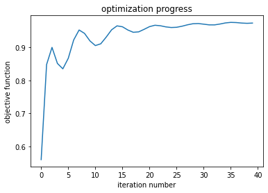
_ = plt.plot(objective_history)
ax = plt.gca()
ax.set_xlabel('iteration number')
ax.set_ylabel('objective function')
ax.set_title('optimization progress')
plt.show()
Next, we can grab our initial and final device from the history lists.
sim_start = make_sim(param_history[0])
data_start = data_history[0]

sim_final = make_sim(param_history[-1])
data_final = data_history[-1]
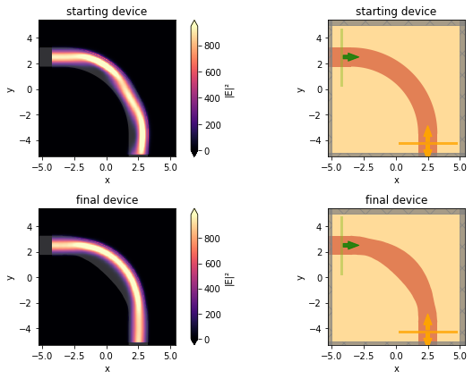
Let's take a look at the final structure. We see that it has a smooth design which is symmetric about the 45 degree angle.
ax = sim_final.plot(z=0.01)
Now let's inspect the difference between the initial and final intensity patterns. We notice that the final device is quite effective at coupling light into the output waveguide! This is especially evident when compared to the starting device.
f, ((ax1, ax2), (ax3, ax4)) = plt.subplots(2, 2, tight_layout=True, figsize=(10, 6))

_ = data_start.plot_field('field', 'E', 'abs^2', ax=ax1)
_ = sim_start.plot(z=0, ax=ax2)
ax1.set_title('starting device')
ax2.set_title('starting device')

_ = data_final.plot_field('field', 'E', 'abs^2', ax=ax3)
_ = sim_final.plot(z=0, ax=ax4)
ax3.set_title('final device')
ax4.set_title('final device')

plt.show()
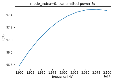
Let's view the transmission now, both in linear and dB scale.
The mode amplitudes are simply an xarray.DataArray that can be selected, post processed, and plotted.
amps = sim_data['mode_bb'].amps.sel(direction="-", mode_index=mode_index)
transmission = abs(amps)**2
transmission_percent = 100 * transmission
transmission_percent.plot(x="f")
ax = plt.gca()
ax.set_title('mode_index=0, transmitted power %')
ax.set_ylabel('T (%)')
plt.show()
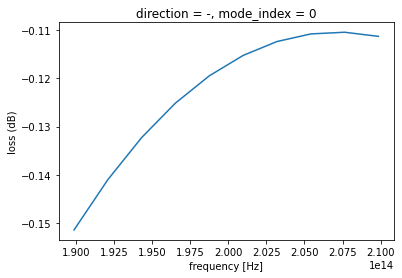
We can also put this in log scale.
loss = 1 - transmission
loss_db = 10 * np.log10(transmission)
loss_db.plot(x="f")
plt.ylabel('loss (dB)')
plt.show()
Finally, let's animate the field pattern evolution over the entire optimization. This will take a minute or so.
import matplotlib.animation as animation
from IPython.display import HTML

fig, (ax1, ax2) = plt.subplots(1, 2, tight_layout=False, figsize=(8, 4))

def animate(i):

    # grab data at iteration "i"
    sim_data_i = data_history[i]

    # plot permittivity
    sim_i = sim_data_i.simulation.to_simulation()[0]
    sim_i.plot_eps(z=0, monitor_alpha=0.0, source_alpha=0.0, ax=ax1)
    # ax1.set_aspect('equal')

    # plot intensity
    int_i = sim_data_i.get_intensity("field")
    int_i.squeeze().plot.pcolormesh(x='x', y='y', ax=ax2, add_colorbar=False, cmap="magma")
    # ax2.set_aspect('equal')

# create animation
ani = animation.FuncAnimation(fig, animate, frames=len(data_history));
plt.close()

# display the animation (press "play" to start)
HTML(ani.to_jshtml())
<Figure size 432x288 with 0 Axes>
To save the animation to file, uncomment the line below. Will take a few minutes to render.
# ani.save('animation_bend_adjoint.gif', fps=60)
MovieWriter ffmpeg unavailable; using Pillow instead.
<Figure size 432x288 with 0 Axes>
Inverse Design: Lecture 5
Here, we continue our discussion of inverse design in photonics and focus on set of optimization techniques that we call “shape optimization”.
Recall that the goal of this process is to design a photonic device for a specific objective. In the previous lectures, we imagined a design region, which was broken into independent pixels. We then optimized the permittivity value in each pixel to meet a give design objective. As discussed, there are many details regarding how to parameterize these permittivity values in order to satisfy fabrication constraints, for example, incorporating minimum feature sizes, binarization, and other factors that ensure that we generate a device that can actually be fabricated. While this is one very important class of optimization problems, there are other ways to set up the problem not necessarily from this pixel-by-pixel perspective.
As an example, imagine that you are trying to design a waveguide taper where there is a narrow waveguide on the left with a mode coming in. You would like to go through a region designed such that the light will couple nicely to the larger waveguide on the right. A conventional design would be to simply put a linear taper in between the narrow waveguide and the wide waveguide. Then, you might want to control the shape of this taper to achieve this objective of mode expansion. In this case, the natural parameters for the optimization would involve the positions of the interface, indicated by the black arrows above. Of course, one could try doing this by pixel-by-pixel optimization, but in many cases, it is perhaps simpler to imagine this in terms of modifying an existing taper design. Such a structure may naturally have a design that satisfies the minimum feature size constraint. Furthermore, we may have some intuition about what the device is trying to achieve based on the more simple and intuitive design. Another advantage is that a regular interface may have lower scattering loss than a pixelated device. In general, there are several advantages to utilizing a geometry-based parameterization rather than a pixelated parameterization if your device allows it.
For a shape-based approach to work, one must be able to compute the derivative of the objective function with respect to the position of the interface using he adjoint method. While we won’t go into much detail here as there are many papers showing how to compute this quantity, it is described in the equation above. The objective you care about is labelled “T” and the parameter describing the interface is given as “s”. The derivative of T with respect to s is computed by performing an integral of both the parallel electric (E) field and the perpendicular displacement (D) field. One needs to handle these different field components separately since they have different boundary conditions across interfaces. Using this formula, you can compute the gradient information with respect to each point along the interface, which can be used to optimize the device with respect to a set of design parameters similar to how we have previously.
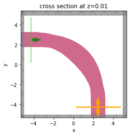
As an example, let’s apply this technique to optimize a waveguide bend. The waveguide geometry is shown above, with a top-down view on the left and a cross section view on the right. The waveguide consists of a silicon nitride region sitting on a silicon dioxide substrate with air above. In this design problem, we’d like to choose the shape of the waveguide to perform a compact, 90-degree bend. The waveguide supports multiple modes, but we inject the fundamental mode on the right hand side. After the light propagates through the waveguide and performs the bend, we want it to couple again to the fundamental mode with high efficiency. We write an objective function with this functionality in mind. The next step is to parameterize the device shape using a set of differentiable parameters.
To parameterize the device, we split it into several sections, drawn above, such that the bend is made up of several rectangular sections. The drawing shows only a few sections for clarity, but in reality, they are chosen to be tightly spaced such that the device is approximately circular. We take as our design parameters the width of each rectangular section along this curve. Thus adjusting the width affects the boundary on both the inner and outer edges. We use the adjoint method to compute the derivative of our objective with respect to this width parameter through the shifting boundary treatment.
As usual, we also want to apply some constraints on this geometry to ensure it can be fabricated. One simple constraint is to make sure that the thickness of each section is neither too large nor too small. To enforce this, one can apply a hyperbolic tangent function to restrict the width of each section to lie between a specified range as the parameters vary continuously. As such, this function will therefore constrain the waveguide to a certain region of space, as shown above. As we have done before, choosing a smooth function makes it possible to take derivatives without worrying about discontinuities.
Another concern for fabrication is the presence of sharp bends in the design. One way to handle this is to impose a penalty for a small radius of curvature in the device and add this penalty to the objective function. To compute this penalty, one may perform a local fit to each set of adjacent points along the device and use an analytical formula to determine an approximate local radius of curvature. Then, again using a smooth function, one can construct a penalty function that is only significant when the local radius of curvature goes below some threshold, labelled “R0” above. Applying this penalty to the objective function has the desired effect of discouraging devices that have sharp features that may be difficult to fabricate.
Here is the visualization of the optimization results incorporating these techniques. On the left are top down views of the device. We can see the performance of the starting device on the top, which clearly does not inject properly into the fundamental output mode, as one can see from the asymmetric intensity pattern at the output interface. On the bottom, we see the final optimized device, which displays smooth features, and injects well into the fundamental output mode as we can see from the symmetric intensity pattern. The objective function as a function of the iteration number is shown on the right hand side and we can see that it gradually improves performance, despite a few oscillations. This final device no longer retains its perfectly circular properties, but clearly provides a substantial improvement in the objective. It is also possible to come up with some intuition based on the final shape, and is clearly more amenable to fabrication than some of the pixelated designs explored earlier.
Finally, here is a short movie of the optimization process. You can see how the boundary between the silicon nitrate and air gets adjusted and how that translates into the measured field distribution inside the waveguide. In summary, this lecture has introduced an alternative to pixel-based approaches to optimization. One can parameterize the device using the interface defined by various geometric parameters and use a modified adjoint method to perform gradient-based optimization using these parameters. For many waveguide problems, this is, in fact, quite an effective strategy for generating a device amenable to nano-fabrication. Furthermore, the devices tend to be easier to understand through human intuition and common ideas in waveguide design.

