TIDY3D
LEARNING CENTER


Inverse Design in Photonics Lecture 4: Fabrication Constraints
By Tyler Hughes, Zongfu Yu and Shanhui FanIn this lecture, we will discuss the need for fabrication constraints in inverse design optimization. We describe one approach to this and demonstrate it by optimizing a Silicon photonics mode converter.
Inverse design optimization of a mode converter using fabrication constraints
To install the
jaxmodule required for this feature, we recommend runningpip install "tidy3d[jax]".
In this notebook, we will use inverse design and the Tidy3D adjoint plugin to create an
integrated photonics component to convert a fundamental waveguide mode to a higher order mode. We introduce
fabrication constraints through a conical filter followed by a tanh projection.
For more details on adjoint optimization, we recommend looking at our previous lectures on inverse design. You can also reference some of the learning materials in our documentation regarding the Tidy3D adjoint plugin.
from typing import List
import numpy as np
import matplotlib.pylab as plt

# import jax to be able to use automatic differentiation
import jax.numpy as jnp
from jax import grad, value_and_grad

# import regular tidy3d
import tidy3d as td
import tidy3d.web as web
from tidy3d.plugins.mode import ModeSolver

# import the components we need from the adjoint plugin
from tidy3d.plugins.adjoint import JaxSimulation, JaxBox, JaxCustomMedium, JaxStructure
from tidy3d.plugins.adjoint import JaxSimulationData, JaxDataArray, JaxPermittivityDataset
from tidy3d.plugins.adjoint.web import run
# parameters in the fabrication constraint parameterization function
BETA = 200
RADIUS = 0.5

# wavelength and frequency
wavelength = 1.55
freq0 = td.C_0 / wavelength
k0 = 2 * np.pi * freq0 / td.C_0

# resolution control
min_steps_per_wvl = 30

# space between boxes and PML
buffer = 1.0 * wavelength

# optimize region size
golden_ratio = 1.618
lx = 5.0
ly = lx / golden_ratio
lz = 0.220
wg_width = 1.0

# num cells
nx = 120
ny = int(nx / golden_ratio)
num_cells = nx * ny

# position of source and monitor (constant for all)
source_x = -lx / 2 - buffer * 0.8
meas_x = lx / 2 + buffer * 0.8

# total size
Lx = lx + 2 * buffer
Ly = ly + 2 * buffer
Lz = lz + 2 * buffer
pml_z = True if Lz else False

# permittivity info
n_si = 3.45
eps_wg = n_si ** 2
eps_deviation_random = 0.5
eps_max = eps_wg
eps_sio2 = 1.44 ** 2
dl = wavelength / min_steps_per_wvl / n_si

# note, we choose the starting permittivities to be uniform with a small, random deviation
params0 =  0.01 * (np.random.random((nx, ny)) - 0.5)

# frequency width and run time
freqw = freq0 / 10
run_time = 50 / freqw

# mode in and out
mode_index_in = 0
mode_index_out = 1
num_modes = max(mode_index_in, mode_index_out) + 1
mode_spec = td.ModeSpec(num_modes=num_modes)
Static Components
Next, we will set up the static parts of the geometry, the input source, and the output monitor using these parameters.
waveguide = td.Structure(
    geometry=td.Box(size=(td.inf, wg_width, lz)), medium=td.Medium(permittivity=eps_wg)
)

substrate = td.Structure(
    geometry=td.Box(
        size=(td.inf, td.inf, Lz),
        center=(0, 0, -Lz/2),
    ),
    medium=td.Medium(permittivity=eps_sio2)
)


mode_size = (0, wg_width * 4, lz * 4)

# source seeding the simulation
forward_source = td.ModeSource(
    source_time=td.GaussianPulse(freq0=freq0, fwidth=freqw),
    center=[source_x, 0, 0],
    size=mode_size,
    mode_index=mode_index_in,
    mode_spec=mode_spec,
    direction="+",
)

# we'll refer to the measurement monitor by this name often
measurement_monitor_name = "measurement"

# monitor where we compute the objective function from
measurement_monitor = td.ModeMonitor(
    center=[meas_x, 0, 0],
    size=mode_size,
    freqs=[freq0],
    mode_spec=mode_spec,
    name=measurement_monitor_name,
)

# field monitor
fld_mnt = td.FieldMonitor(
    center=(0,0,0),
    size=(td.inf, td.inf, 0),
    freqs=[freq0],
    name="field",
)
[12:37:04] WARNING: Default value for the field monitor           monitor.py:261
           'colocate' setting has changed to 'True' in Tidy3D
           2.4.0. All field components will be colocated to the
           grid boundaries. Set to 'False' to get the raw fields
           on the Yee grid instead.
Input Structures
Next, we write a function to return the pixellated array of permittivity values given our parameters using JaxCustomMedium.
We'll first apply a ConicFilter to the raw parameters and then apply a BinaryProjector to give the permittivity values.
We will feed the result of this function to our JaxSimulation.input_structures and will take the
gradient w.r.t. the inputs.
from tidy3d.plugins.adjoint.utils.filter import ConicFilter, BinaryProjector

def make_input_structures(params: jnp.array) -> List[JaxStructure]:

    size_box_x = float(lx) / nx
    size_box_y = float(ly) / ny
    size_box = (size_box_x, size_box_y, lz)

    x0_min = -lx / 2 + size_box_x / 2
    y0_min = -ly / 2 + size_box_y / 2

    input_structures = []

    coords_x = [x0_min + index_x * size_box_x - 1e-5 for index_x in range(nx)]
    coords_y = [y0_min + index_y * size_box_y - 1e-5 for index_y in range(ny)]

    coords = dict(x=coords_x, y=coords_y, z=[0], f=[freq0])

    if RADIUS:
        conic_filter = ConicFilter(radius=RADIUS, design_region_dl=size_box_x)
        params = conic_filter.evaluate(params)

    params_01 = 0.5 * (jnp.tanh(params * BETA) + 1.0)
    params = (eps_wg - 1) * params_01 + 1.05
    params = params.reshape((nx, ny, 1, 1))

    field_components = {
        f"eps_{dim}{dim}": JaxDataArray(values=params, coords=coords) for dim in "xyz"
    }
    eps_dataset = JaxPermittivityDataset(**field_components)
    custom_medium = JaxCustomMedium(eps_dataset=eps_dataset)
    box = JaxBox(center=(0, 0, 0), size=(lx, ly, lz))
    custom_structure = JaxStructure(geometry=box, medium=custom_medium)
    return [custom_structure]
Jax Simulation
Next, we write a function to return the JaxSimulation as a function of our parameters.
We make sure to add the pixellated JaxStructure list to input_structures and the
measurement_monitor to output_monitors.
def make_sim(params) -> JaxSimulation:

    input_structures = make_input_structures(params)

    return JaxSimulation(
        size=[Lx, Ly, Lz],
        grid_spec=td.GridSpec.auto(min_steps_per_wvl=min_steps_per_wvl),
        structures=[waveguide, substrate],
        input_structures=input_structures,
        sources=[forward_source],
        monitors=[fld_mnt],
        output_monitors=[measurement_monitor],
        run_time=run_time,
        subpixel=True,
        boundary_spec=td.BoundarySpec.pml(x=True, y=True, z=pml_z),
        shutoff=1e-8,
        courant=0.9,
    )
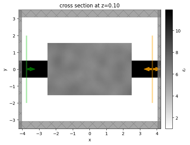
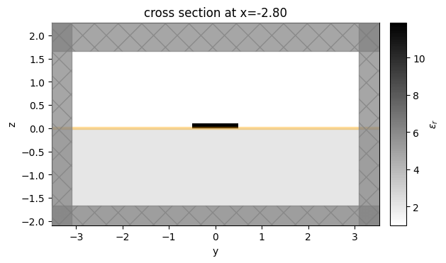
Visualize
Let's visualize the simulation to see how it looks
sim_start = make_sim(params0)

ax = sim_start.plot_eps(z=0.1)
ax = sim_start.plot_eps(x=-2.8)

plt.show()
Select Input and Output Modes
Next, let's visualize the mode profiles so we can inspect which mode indices we want to inject and transmit.
mode_solver = ModeSolver(
    simulation=sim_start, plane=forward_source, mode_spec=mode_spec, freqs=[freq0]
)
modes = mode_solver.solve()

print("Effective index of computed modes: ", np.array(modes.n_eff))

fig, axs = plt.subplots(num_modes, 3, figsize=(10, 12), tight_layout=True)
for mode_ind in range(num_modes):
    for field_ind, field_name in enumerate(("Ex", "Ey", "Ez")):
        field = modes.field_components[field_name].sel(mode_index=mode_ind)
        ax = axs[mode_ind, field_ind]
        field.real.plot(ax=ax)
        ax.set_title('')
[12:37:05] WARNING: Use the remote mode solver with subpixel  mode_solver.py:154
           averaging for better accuracy through
           'tidy3d.plugins.mode.web.run(...)'.
Effective index of computed modes: [[2.0610273 1.6198782]]
![Effective index of computed modes: [[2.0610273 1.6198782]]](/assets/images/inverse-design/Lecture_04/Python_Tutorial_04_3.png)
Aftert inspection, we decide to inject the fundamental, Ey-polarized input into the 1st order Ey-polarized input.
From the plots, we see that these modes correspond to the first and third rows, or mode_index=0
and mode_index=1, respectively.
So we make sure that the mode_index_in and mode_index_out variables are set
appropriately.
Post Processing
We will define one more function to tell us how we want to postprocess a JaxSimulationData
object to give the conversion power that we are interested in maximizing.
def measure_power(sim_data: JaxSimulationData) -> float:
    """Return the power in the output_data amplitude at the mode index of interest."""
    output_amps = sim_data[measurement_monitor_name].amps
    amp = output_amps.sel(direction="+", f=freq0, mode_index=mode_index_out)
    return jnp.sum(jnp.abs(amp) ** 2)
Define Objective Function
Finally, we need to define the objective function that we want to maximize as a function of our input parameters that returns the conversion power. This is the function we will differentiate later.
def J(params, step_num: int = None, verbose: bool = False) -> float:
    sim = make_sim(params)
    task_name = "inv_des"
    if step_num:
        task_name += f"_step_{step_num}"
    sim_data = run(sim, task_name=task_name, verbose=verbose)
    return measure_power(sim_data), sim_data
Inverse Design
Now we are ready to perform the optimization.
We use the jax.value_and_grad function to get the gradient of J with respect to the
permittivity of each Box, while also returning the converted power associated with the current
iteration, so we can record this value for later.
Let's try running this function once to make sure it works.
dJ_fn = value_and_grad(J, has_aux=True)
(val, data), grad = dJ_fn(params0, verbose=True)
print(grad.shape)
           View task using web UI at                               webapi.py:190
           'https://tidy3d.simulation.cloud/workbench?taskId=fdve-
           70c431fe-b001-4bd0-9362-bf0d41a56b7bv1'.
Output()
Output()
Output()
Output()
Output()
Output()
           View task using web UI at                               webapi.py:190
           'https://tidy3d.simulation.cloud/workbench?taskId=fdve-
           1c041d20-85bf-40c1-a785-81bfdabf2aaav1'.
Output()
Output()
Output()
Output()
Output()
Output()
(120, 74)
val
Array(0.00057049, dtype=float32)
Optimization
We will use "Adam" optimization strategy to perform sequential updates of each of the permittivity values in the JaxCustomMedium.
For more information on what we use to implement this method, see this article.
We will run 10 steps and measure both the permittivities and powers at each iteration.
We capture this process in an optimize function, which accepts various parameters that we can
tweak.
import optax

td.config.logging_level = "ERROR"

# hyperparameters
num_steps = 50
learning_rate = 25e-4

# initialize adam optimizer with starting parameters
params = np.array(params0)
optimizer = optax.adam(learning_rate=learning_rate)
opt_state = optimizer.init(params)

# store history
Js = []
params_history = [params]
data_history = [data]

for i in range(num_steps):

    # compute gradient and current objective funciton value
    (value, data), gradient = dJ_fn(params, step_num=i+1)

    # outputs
    print(f"step = {i + 1}")
    print(f"\tJ = {value:.4e}")
    print(f"\tgrad_norm = {np.linalg.norm(gradient):.4e}")

    # compute and apply updates to the optimizer based on gradient (-1 sign to maximize obj_fn)
    updates, opt_state = optimizer.update(-gradient, opt_state, params)
    params = optax.apply_updates(params, updates)

    # save history
    Js.append(value)
    params_history.append(params)
    data_history.append(data)
step = 1
	J = 5.7048e-04
	grad_norm = 7.1980e-01
step = 2
	J = 5.8271e-02
	grad_norm = 3.2094e+00
step = 3
	J = 1.8351e-01
	grad_norm = 6.5283e+00
step = 4
	J = 2.9831e-01
	grad_norm = 6.8098e+00
step = 5
	J = 3.7441e-01
	grad_norm = 4.5694e+00
step = 6
	J = 2.5480e-01
	grad_norm = 4.0456e+00
step = 7
	J = 2.8951e-01
	grad_norm = 3.4236e+00
step = 8
	J = 3.6417e-01
	grad_norm = 2.4072e+00
step = 9
	J = 4.0927e-01
	grad_norm = 1.4756e+00
step = 10
	J = 4.0717e-01
	grad_norm = 2.1635e+00
step = 11
	J = 4.0322e-01
	grad_norm = 2.7579e+00
step = 12
	J = 4.2978e-01
	grad_norm = 2.5637e+00
step = 13
	J = 4.7454e-01
	grad_norm = 1.8433e+00
step = 14
	J = 5.1639e-01
	grad_norm = 1.4946e+00
step = 15
	J = 5.5091e-01
	grad_norm = 1.1112e+00
step = 16
	J = 5.5076e-01
	grad_norm = 1.3412e+00
step = 17
	J = 5.4971e-01
	grad_norm = 1.5222e+00
step = 18
	J = 5.5867e-01
	grad_norm = 1.5042e+00
step = 19
	J = 5.7811e-01
	grad_norm = 1.3299e+00
step = 20
	J = 6.0190e-01
	grad_norm = 1.1056e+00
step = 21
	J = 6.2367e-01
	grad_norm = 8.8847e-01
step = 22
	J = 6.3966e-01
	grad_norm = 7.7817e-01
step = 23
	J = 6.5028e-01
	grad_norm = 8.4007e-01
step = 24
	J = 6.5917e-01
	grad_norm = 9.3976e-01
step = 25
	J = 6.6967e-01
	grad_norm = 9.3501e-01
step = 26
	J = 6.7108e-01
	grad_norm = 1.0764e+00
step = 27
	J = 6.7766e-01
	grad_norm = 1.0326e+00
step = 28
	J = 6.8828e-01
	grad_norm = 8.3363e-01
step = 29
	J = 6.9897e-01
	grad_norm = 5.4822e-01
step = 30
	J = 7.0591e-01
	grad_norm = 3.2599e-01
step = 31
	J = 7.0780e-01
	grad_norm = 4.5388e-01
step = 32
	J = 7.0682e-01
	grad_norm = 6.5268e-01
step = 33
	J = 7.0634e-01
	grad_norm = 7.0469e-01
step = 34
	J = 7.0759e-01
	grad_norm = 6.5637e-01
step = 35
	J = 7.0991e-01
	grad_norm = 6.0179e-01
step = 36
	J = 7.0695e-01
	grad_norm = 8.4391e-01
step = 37
	J = 7.0813e-01
	grad_norm = 7.4822e-01
step = 38
	J = 7.1192e-01
	grad_norm = 6.5498e-01
step = 39
	J = 7.1648e-01
	grad_norm = 7.1992e-01
step = 40
	J = 7.2240e-01
	grad_norm = 5.7227e-01
step = 41
	J = 7.2778e-01
	grad_norm = 4.7710e-01
step = 42
	J = 7.3241e-01
	grad_norm = 4.8525e-01
step = 43
	J = 7.3685e-01
	grad_norm = 3.3807e-01
step = 44
	J = 7.3971e-01
	grad_norm = 3.6552e-01
step = 45
	J = 7.4169e-01
	grad_norm = 5.4077e-01
step = 46
	J = 7.4515e-01
	grad_norm = 5.1662e-01
step = 47
	J = 7.4963e-01
	grad_norm = 3.8266e-01
step = 48
	J = 7.5354e-01
	grad_norm = 3.8529e-01
step = 49
	J = 7.5739e-01
	grad_norm = 4.5926e-01
step = 50
	J = 7.6220e-01
	grad_norm = 4.4518e-01
params_after = params_history[-1]
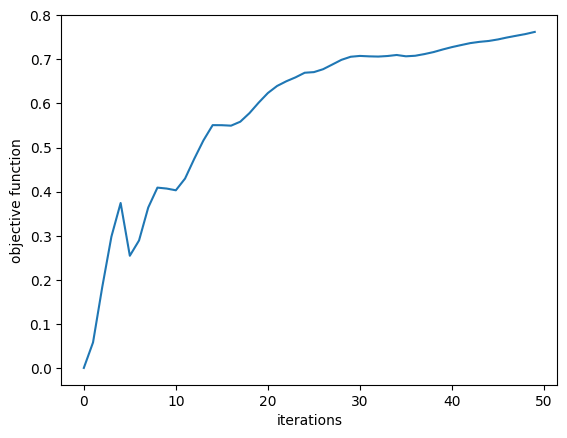
Results
First, we plot the objective function as a function of step and notice that it converges nicely!
plt.plot(jnp.array(Js))
plt.xlabel("iterations")
plt.ylabel("objective function")

plt.show()
Js
[Array(0.00057048, dtype=float32),
 Array(0.05827059, dtype=float32),
 Array(0.18350816, dtype=float32),
 Array(0.29830727, dtype=float32),
 Array(0.3744134, dtype=float32),
 Array(0.25479904, dtype=float32),
 Array(0.2895097, dtype=float32),
 Array(0.36417153, dtype=float32),
 Array(0.4092735, dtype=float32),
 Array(0.4071658, dtype=float32),
 Array(0.40322325, dtype=float32),
 Array(0.42977965, dtype=float32),
 Array(0.4745363, dtype=float32),
 Array(0.5163853, dtype=float32),
 Array(0.55091274, dtype=float32),
 Array(0.5507563, dtype=float32),
 Array(0.54970896, dtype=float32),
 Array(0.55866563, dtype=float32),
 Array(0.57811373, dtype=float32),
 Array(0.6018991, dtype=float32),
 Array(0.6236749, dtype=float32),
 Array(0.6396642, dtype=float32),
 Array(0.650282, dtype=float32),
 Array(0.659171, dtype=float32),
 Array(0.6696716, dtype=float32),
 Array(0.6710839, dtype=float32),
 Array(0.67766047, dtype=float32),
 Array(0.6882825, dtype=float32),
 Array(0.6989677, dtype=float32),
 Array(0.70590943, dtype=float32),
 Array(0.70780003, dtype=float32),
 Array(0.7068219, dtype=float32),
 Array(0.70633996, dtype=float32),
 Array(0.70758593, dtype=float32),
 Array(0.70990896, dtype=float32),
 Array(0.70695156, dtype=float32),
 Array(0.7081289, dtype=float32),
 Array(0.71192354, dtype=float32),
 Array(0.7164821, dtype=float32),
 Array(0.7223976, dtype=float32),
 Array(0.72777903, dtype=float32),
 Array(0.73240846, dtype=float32),
 Array(0.7368534, dtype=float32),
 Array(0.73971343, dtype=float32),
 Array(0.74168736, dtype=float32),
 Array(0.7451518, dtype=float32),
 Array(0.749627, dtype=float32),
 Array(0.7535403, dtype=float32),
 Array(0.7573899, dtype=float32),
 Array(0.7621993, dtype=float32)]
print(f"Initial power conversion = {Js[0]*100:.2f} %")
print(f"Final power conversion = {Js[-1]*100:.2f} %")
Initial power conversion = 0.06 %
Final power conversion = 76.22 %
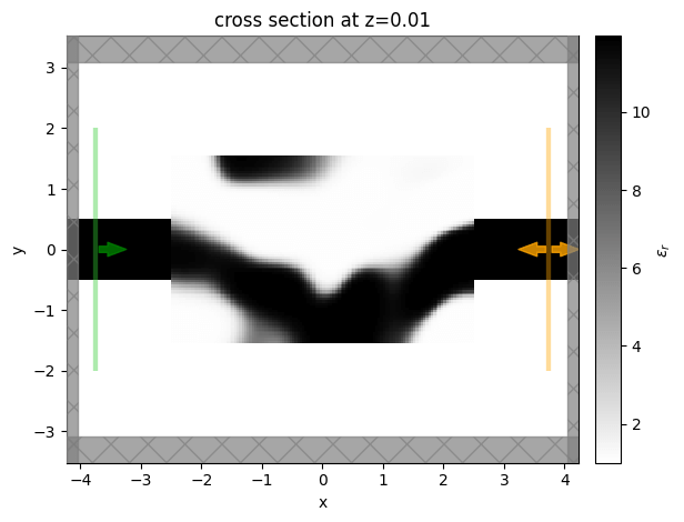
We then will visualize the final structure, so we convert it to a regular Simulation using the
final permittivity values and plot it.
sim_final = make_sim(params_after)
sim_data_final = data_history[-1]
sim_final = sim_data_final.simulation
sim_final = sim_final.to_simulation()[0]
sim_final.plot_eps(z=0.01)
plt.show()
Finally, we want to inspect the fields, so we add a field monitor to the Simulation and perform
one more run to record the field values for plotting.
f, (ax1, ax2) = plt.subplots(2, 1, figsize=(15, 6))
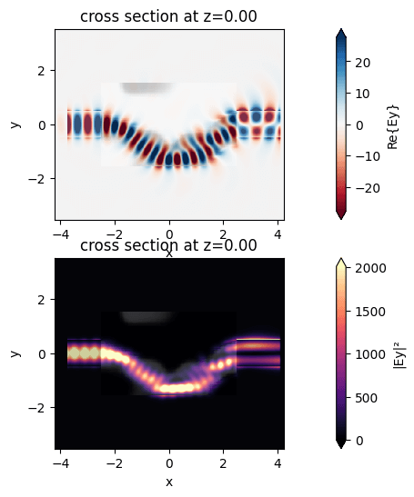
ax1 = sim_data_final.plot_field("field", "Ey", z=0, ax=ax1)
ax2 = sim_data_final.plot_field("field", "Ey", "abs^2", z=0, ax=ax2)
plt.show()
import matplotlib.animation as animation
from IPython.display import HTML

fig, (ax1, ax2) = plt.subplots(1, 2, tight_layout=False, figsize=(8, 4))

def animate(i):

    # grab data at iteration "i"
    sim_data_i = data_history[i]

    # plot permittivity
    sim_i = sim_data_i.simulation.to_simulation()[0]
    sim_i.plot_eps(z=lz/2, monitor_alpha=0.0, source_alpha=0.0, ax=ax1)
    # ax1.set_aspect('equal')

    # plot intensity
    # int_i = sim_data_i.get_intensity("field")
    # int_i.squeeze().plot.pcolormesh(x='x', y='y', ax=ax2, add_colorbar=True, cmap="magma")
    abs(sim_data_i["field"].Ey**2).plot(x='x', y='y', ax=ax2, add_colorbar=False, cmap="magma")
    # ax2.set_aspect('equal')

# create animation
ani = animation.FuncAnimation(fig, animate, frames=len(data_history));
plt.close()

# display the animation (press "play" to start)
HTML(ani.to_jshtml())
<Figure size 640x480 with 0 Axes>
ani.save('animation_best.gif', writer='imagemagick', fps=60)
MovieWriter imagemagick unavailable; using Pillow instead.
<Figure size 640x480 with 0 Axes>
Inverse Design: Lecture 4
In this lecture, we will continue our discussion on inverse design in photonics. Here we will describe a technique that allows us to incorporate basic feature constraints.
As a brief review, last time we gave a simple demo of using inverse design to make a lens. In this design, we have a source and a desired focusing spot. The goal is then to design the region in between such that the wave generated by the source will be focused in the intended focusing region. The design was achieved by simply adjusting the value of the relative permittivty at each point inside the design region. From the animation, one can see that it works reasonably well as, with a few iterations, it can accomplish the desired focusing behavior. However, in reality, there is a lot more that you need to do to produce a design that satisfies fabrication constraints, which we will be discussing in these slides.
To start, let’s discuss what kind of fabrication constraints you may typically encounter. In silicon photonics, for example, one might design devices by etching a thin film of silicon. In the image above we show one such device comprising of a a silicon ring coupled to a waveguide. The resulting device therefore contains regions of only silicon and air. Therefore, in our inverse design process, there are technically only two possible permittivity values that should be allowed in our final device: that of silicon and that of air. This fact needs to be taken into account in the optimization algorithm to produce a structure that can be fabricated. In fact, there many other fabrication constraints one might apply to this process. For example, if your structure is defined using photolithography, there may be a minimum feature size that one can reliably produce depending on the fabrication technique, which must be taken into account as well. In general, one needs to consider all of these effects when designing the photonic device to ensure the final device is usable.
We will use a mode converter as a simple device to illustrate how to incorporate some of these concepts into our design algorithm. The mode converter consists of an input waveguide connected to an output waveguide, both support multiple modes. The intent of the device is to convert one eigenmode of the input waveguide to another eigenmode of the output waveguide with as high of an efficiency as possible. One can attempt to accomplish this by placing a “design region” between the two waveguides to produce the desired conversion. In the silicon photonics context, this design region would consist of a thin silicon film sitting on top of the silicon dioxide substrate that can be etched with a desired pattern. The goal, therefore is to find the pattern to etch such that the design region still consists of air and silicon but is able to convert the two modes as required. To be more specific, we can define the objective function to maximize as the overlap integral between the actual measured output waveguide field pattern and that of the desired mode.
Now, one can apply the same approach as we’ve shown in previous lectures to directly modify the relative permittivity of the design region using the gradient of this cost function. This approach will produce a design that works to convert modes, as we can see by the field intensity plot on the top right. In this plot, we are exciting the even fundamental mode of the input waveguide on the left hand side, and the output waveguide shows that we are exciting the first high order mode on the right hand side, which is clearly odd. However, looking at the structure that produced this functionality, one can clearly see that it is has a continuous variation from the permittivity of air to the permittivity of silicon. In this sense, it would not be possible to fabricate such a device using our etching technique. Moreover, we would ideally like to have a feature size that is large enough to be able to etch with the resolution afforded to us by our fabrication process.
To incorporate these kinds of fabrication constraints more generally, the key insight is that one should not directly optimize the relative permittivity. Instead, one can imagine a function that takes the parameters and generates the relative permittivity as its output. One can then craft this function to incorporate any feature size constraint that you care about. For example, one can modify this function to incorporate operations that bias the structure towards being one of two permittivity values (binarization) or feature size constraints.
Before discussing the specifics of this function, it is important to point out that we must ensure that it is smooth and differentiable. The reason is that when we want to optimize this device through gradient-based methods, we need to be able to compute the gradient of our objective function with respect to the raw parameter values. The adjoint method gives us a way to do this, but it requires us being able to propagate the derivative information backwards through our device parameterization function. Therefore, the derivative of this function must be well-defined for us to optimize in our parameter space.
To illustrate the points we’ve discussed so far, let’s introduce one method for binarization of our device. Let’s imagine our parameter values (p) can range between negative infinity and infinity, with p=0 representing the halfway point between our two limits of the permittivity. We can introduce a hyperbolic tangent function to convert between parameter values and permittivity values. The function has an extra parameter “beta”, which controls the “steepness” of the projection. On the right hand side, we plot the tanh function with varying values of beta and see that for small beta, the projection is almost linear. However, as beta increases, it begins to look like a step function. A high beta value therefore has the effect of applying binarization to our device and one can tune this parameter either during or after optimization to help produce a binary structure. In short, the gradient-based optimization will still tune parameters in the parameter space, but passing the values through this tanh function will result in more binarized permittivity values.
To illustrate this effect, here are the results of three optimizations with different values of beta in the tanh projection. As we can see, increasing the beta has the effect of creating more binarized structures, whereas the low beta structures tend to have permittivities between that of air and silicon. From looking at the field plots, we also notice that all three structures successfully perform the mode conversion. While this is an important first step, we still notice that the permittivity of the binarized structure varies rapidly from pixel to pixel. Therefore it would be very difficult to actually fabricate such a structure without introducing some kind of constraint on the feature size.
To introduce feature size constraints, we will add another process to the pipeline of mapping from parameter space to the permittivity values in our device. We now imagine a two step process, we still have a parameter space that can vary pixel-by-pixel. However, before passing through our hyperbolic tangent projection function, we will first convolve our parameters with a kernel so that we can “smooth” the values in real space a bit. We choose a kernel with a radius R, where the larger R produces more smoothed out values, producing larger feature size. Through this parameter, one can therefore control how large of feature size is present in the final device. As we discussed, both of these functions are smooth and differentiable, so it is possible to pass gradient information backwards through this mapping for optimization.
Here are some results of optimizing the mode converter with three values of R. When R=0, we notice that the results are very pixelated, with extremely small feature size. As R increases to 100nm, we start to see larger feature sizes, which get even larger as we further increase R. Again, all three devices seem to convert modes as desired based on their field profiles.
Here we apply the procedure we’ve layed out on a three dimensional optimization problem. We set up our device as a thin film of silicon on a silicon dioxide substrate and optimize the pattern etched onto the silicon in the design region. We introduce a conic filter with radius of 500nm and a tanh projection with beta=200. We show the top view of the structure and the field patterns after 50 iterations of optimization. The final device works as intended to convert the waveguide modes and also exhibits large feature size and mostly binarized permittivity values.
To summarize, an important idea to incorporate fabrication constraints in inverse design is to imagine a mapping from your optimization parameter space to your structure. One can then craft this parameterization to incorporate any of the constraints that you might care about in your application. Of course, in this simple example, we introduced some basic constraints, but there are a lot of degrees of freedom that could be introduced so one must think carefully about such choice of parameterization. In future lectures we will go into more details about these considerations.

