FDTD Simulations in Cutting-Edge Photonics: From Novel 2D Materials to Quantum Technologies and Consumer Electronics
The Finite-Difference Time-Domain (FDTD) method is a computational modeling technique widely used in the field of photonics. FDTD has significantly changed the way researchers study and predict the behavior of electromagnetic waves. This review article delves into the recent applications of FDTD simulations in cutting-edge photonics research and engineering. Specifically, it showcases examples of the use of FDTD simulations in areas such as novel 2D materials (such as graphene and transition-metal dichalcogenides), quantum technologies (like quantum dots and single photon light extraction), and consumer-grade electronics (such as CMOS image sensors).
2D materials in photonics
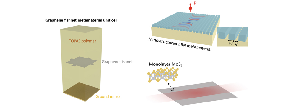
The emergence of 2D materials represents a significant breakthrough. These ultra-thin materials, often mere atoms in thickness, demonstrate unique electronic, optical, and mechanical properties, markedly different from their bulk forms. Graphene, a monolayer of carbon atoms in a honeycomb lattice, exemplifies this with its exceptional conductivity and transparency. Beyond graphene, 2D materials like TMDs, black phosphorus, and hexagonal boron nitride (hBN) have been identified, each with distinctive optical properties. These materials have facilitated novel applications in photonics, including ultrafast photodetectors, flexible optoelectronics, advanced photovoltaic cells, and light-emitting diodes (LEDs). The nanoscale manipulation of light using these 2D materials paves the way for innovative developments in communication technologies, energy harvesting, and quantum computing, marking a transformative phase in photonics.
Our example library showcases various photonic devices that are integrated with 2D materials. Some examples include the graphene metamaterial absorber, the nanostructured hBN with hyperbolic polaritons, and the waveguide made of MoS2 monolayer.
Photonic components for next-gen quantum technology
The rapid advancement of quantum technology is significantly influenced by the development of sophisticated photonic components, essential for driving the next generation of quantum systems. These components, encompassing single-photon sources, detectors, and integrated photonic circuits, form the foundation of quantum communication, computing, and sensing. They enable precise photon manipulation and control, facilitating critical quantum phenomena such as entanglement and superposition. In quantum computing, photonic elements are instrumental in generating and manipulating qubits, the quantum bits that exist in multiple states simultaneously, thereby significantly enhancing computing capabilities. In quantum communication, these components are crucial for establishing highly secure channels through quantum key distribution (QKD). Furthermore, progress in integrated quantum photonics is leading to more compact and robust quantum devices, advancing their practical application in various sectors, including secure data transmission and high-precision measurements. As ongoing research pushes the limits of current technology, photonic components are poised to be key in harnessing the full potential of quantum technology, ushering in a new era of information processing and other applications.
Our example library features several quantum photonics-related examples, including the Bullseye cavity quantum emitter light extractor, the inverse-designed quantum emitter light extractor, and the Plasmonic Yagi-Uda nanoantenna.

Photonic devices in consumer-grade electronics
The integration of advanced photonic devices in consumer electronics is markedly enhancing user experiences, as seen in the use of CMOS image sensors in digital imaging as well as Fresnel lenses and diffractive gratings in augmented reality (AR) and virtual reality (VR) systems. CMOS sensors, notable for their low power consumption and high-quality imaging, are crucial in smartphones and digital cameras, capturing high-resolution images with excellent clarity and color fidelity. These sensors utilize photonics to convert light into electronic signals, resulting in the vivid, detailed digital images prevalent in modern devices. In AR and VR, Fresnel lenses, known for their concentric ring structure, offer a lightweight, thin alternative to traditional lenses, ideal for compact headsets. They effectively bend light for immersive visual experiences while reducing headset bulk, enhancing user comfort during prolonged use. CMOS image sensors and Fresnel lenses demonstrate the significant role of photonic technologies in consumer electronics, driving innovation and expanding the possibilities of user interaction in digital environments.

Conclusion
The advancements in technology have led to a significant increase in the demand for faster and more efficient computing methods. Photonic devices are becoming increasingly important in modern technology, and the demand for faster and more accurate electromagnetic simulations is growing. FDTD has been a critical tool in advancing the development of photonic devices, but conventional FDTD solvers can no longer keep up with the speed of technological development. Novel hardware-accelerated FDTD tools like Tidy3D are designed to overcome the limitations of traditional FDTD solvers. These tools leverage the power of modern computing hardware to deliver faster and more accurate simulations, making it possible to design and optimize photonic devices at a scale and speed that was previously impossible. With the advent of these innovative tools, a new era of photonic device development is emerging, one that promises to deliver faster, more efficient, and more reliable technology.